
Electric element-embedded multilayer substrate and method for manufacturing the same

a technology of multi-layer substrates and components, applied in the direction of printed circuits, printed circuit non-printed electric components association, semiconductor/solid-state device details, etc., can solve problems such as damage to the electric element itself and disconnection of a wire pattern from the electric element, so as to reduce or prevent damage to the electric element and prevent the disconnection of a wire pattern

Active Publication Date: 2017-07-04
MURATA MFG CO LTD
View PDF12 Cites 0 Cited by
  • Summary
  • Abstract
  • Description
  • Claims
  • Application Information

AI Technical Summary

Benefits of technology

The present invention provides an electric element-embedded multilayer substrate that can protect the embedded electric element and prevent damage or disconnection of its wires, even under stress, such as impact or bending. Additionally, the invention includes a manufacturing method for this substrate.

Problems solved by technology

By the action of the stress transferred to the electric element, defects such as damage to the electric element itself and disconnection of a wire pattern from the electric element may be caused.

Method used


Image

  • Electric element-embedded multilayer substrate and method for manufacturing the same
  • Electric element-embedded multilayer substrate and method for manufacturing the same
  • Electric element-embedded multilayer substrate and method for manufacturing the same

Examples


embodiment 1

Preferred Embodiment 1

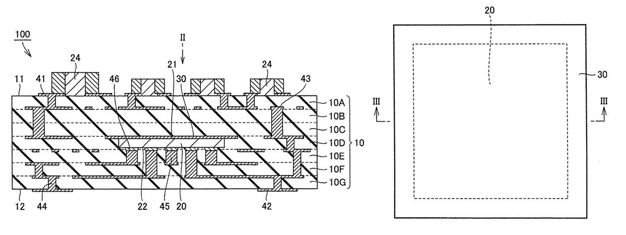
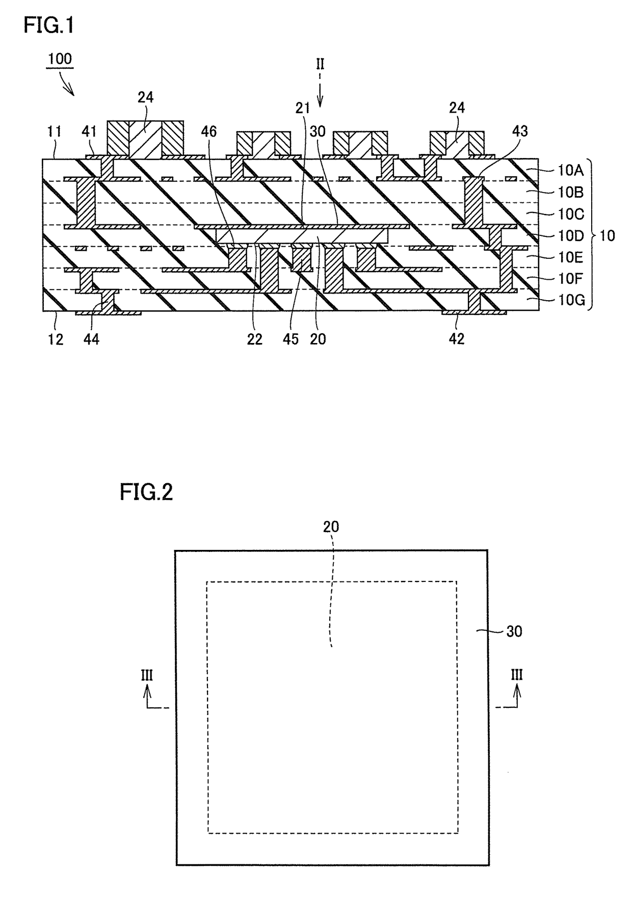
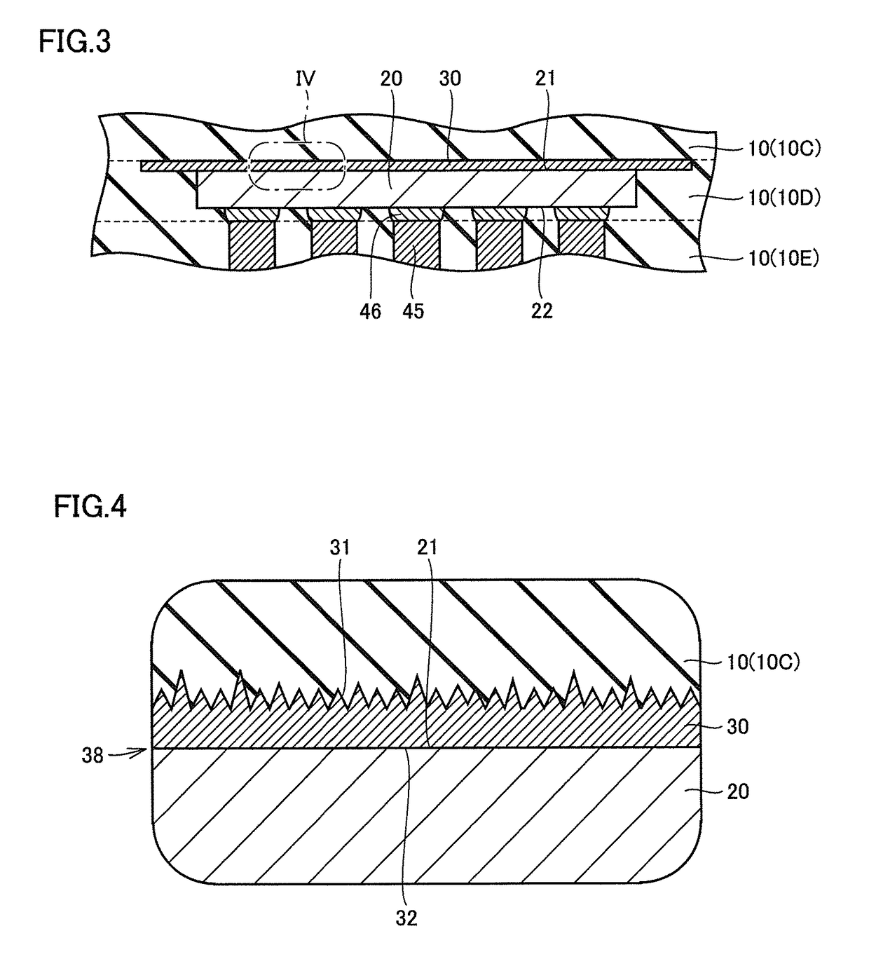
[0038]An electric element-embedded multilayer substrate 100 in accordance with a first preferred embodiment of the present invention (Preferred Embodiment 1) will be described with reference to FIG. 1. FIG. 1 is a cross sectional view showing the electric element-embedded multilayer substrate 100. The electric element-embedded multilayer substrate 100 includes a multilayer substrate 10, an active element 20 (electric element), passive elements 24, and a slide member 30.

[0039]The multilayer substrate 10 is preferably defined by stacking a plurality of base material layers 10A to 10G having flexibility. The multilayer substrate 10 itself also has flexibility. Base material layers 10A to 10G are preferably, for example, sheets of thermoplastic resin such as, for example, polyimide or a liquid crystal polymer, as members having a flexibility higher than that of the active element 20 embedded in multilayer substrate 10 (detail will be described later).

[0040]A liquid...

embodiment 2

Preferred Embodiment 2

[0074]An electric element-embedded multilayer substrate 100A in a second preferred embodiment of the present invention (Preferred Embodiment 2) will now be described with reference to FIG. 11. FIG. 11 is a cross sectional view showing the electric element-embedded multilayer substrate 100A. The electric element-embedded multilayer substrate 100A preferably includes a multilayer substrate 10, an active element 20, passive elements 24, another active element 28, a slide member 30, and an auxiliary member 36. The other active element 28 is preferably mounted on a front surface 11 of multilayer substrate 10.

[0075]The auxiliary member 36 is preferably arranged opposite to the slide member 30 with base material layer 10E being sandwiched therebetween. The auxiliary member 36 is preferably arranged adjacent to the slide member 30 in the direction in which base material layers 10A to 10G are stacked. The auxiliary member 36 can be defined by a sheet metal disposed on a...


PUM

PropertyMeasurementUnit
electricaaaaaaaaaa
surface roughnessaaaaaaaaaa
thermoplasticityaaaaaaaaaa

Abstract

An electric element-embedded multilayer substrate, which is a multilayer substrate including an electric element embedded therein and a plurality of base material layers having flexibility, the electric element including a main surface and being embedded in the multilayer substrate to be sandwiched between the base material layers, and a slide member provided between the main surface of the electric element and the base material layer.

Description

BACKGROUND OF THE INVENTION[0001]1. Field of the Invention[0002]The present invention relates to an electric element-embedded multilayer substrate, which is a multilayer substrate including an electric element embedded therein, and a method for manufacturing the same.[0003]2. Description of the Related Art[0004]Various types of electronic equipment, such as a mobile phone, tend to be downsized. Accordingly, electric elements such as circuit elements defining electronic equipment also tends to be downsized. Under such a circumstance, an electric element such as a circuit element is mounted on and integrated with a multilayer substrate, and used as an electric element-integrated multilayer substrate.[0005]A typical electric element-integrated multilayer substrate 100Y will be described with reference to FIG. 13. Electric element-integrated multilayer substrate 100Y includes a multilayer substrate 10 formed by stacking a plurality of base material layers. In-plane wires 43 and interlay...

Claims


Application Information

Patent Timeline
Patent Type & Authority Patents(United States)
IPC IPC(8): H05K1/18H05K1/02H01L23/538H05K3/46H01L23/498
CPCH05K1/0271H01L23/5389H05K1/186H05K1/188H05K3/4617H05K3/4644H01L23/49822H01L2224/16225H01L2924/19105H05K1/0206H05K3/4632H05K3/4635H05K2201/0141H05K2201/09781H05K2201/10674Y10T29/4913Y10T29/49139
Inventor KATO, NOBORUOZAWA, MASAHIRO
Owner MURATA MFG CO LTD
Learn More