
Semiconductor device including dummy contact

a technology of dummy contact and semiconductor devices, which is applied in the direction of semiconductor devices, semiconductor/solid-state device details, electrical apparatus, etc., can solve the problems of increasing the difficulty of forming contact plugs and interconnections, and the possibility of generating various defects in single damascene process, so as to reduce the defect in the interconnection process and high integration

Active Publication Date: 2021-02-16
SAMSUNG ELECTRONICS CO LTD
View PDF29 Cites 0 Cited by
  • Summary
  • Abstract
  • Description
  • Claims
  • Application Information

AI Technical Summary

Benefits of technology

The patent text is about a new semiconductor device and method of making it that can help reduce defects during the process of connecting components and achieve higher levels of integration.

Problems solved by technology

A process of forming contact plugs and interconnections is becoming increasingly difficult, for example owing to high integration of semiconductor devices.
The single damascene process may generate various defects, such as dishing, due to the arrangement of the contact plugs.

Method used


Image

  • Semiconductor device including dummy contact
  • Semiconductor device including dummy contact
  • Semiconductor device including dummy contact

Examples


Embodiment Construction

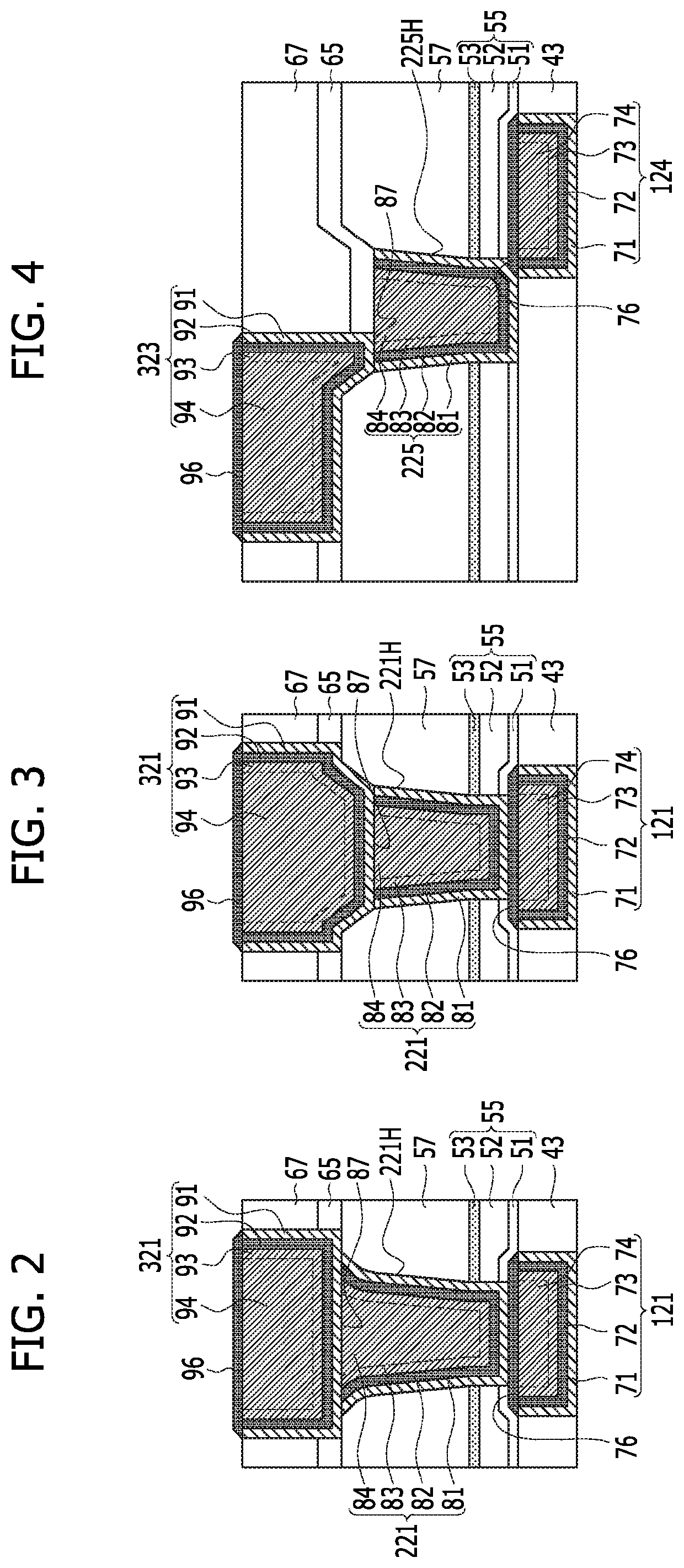
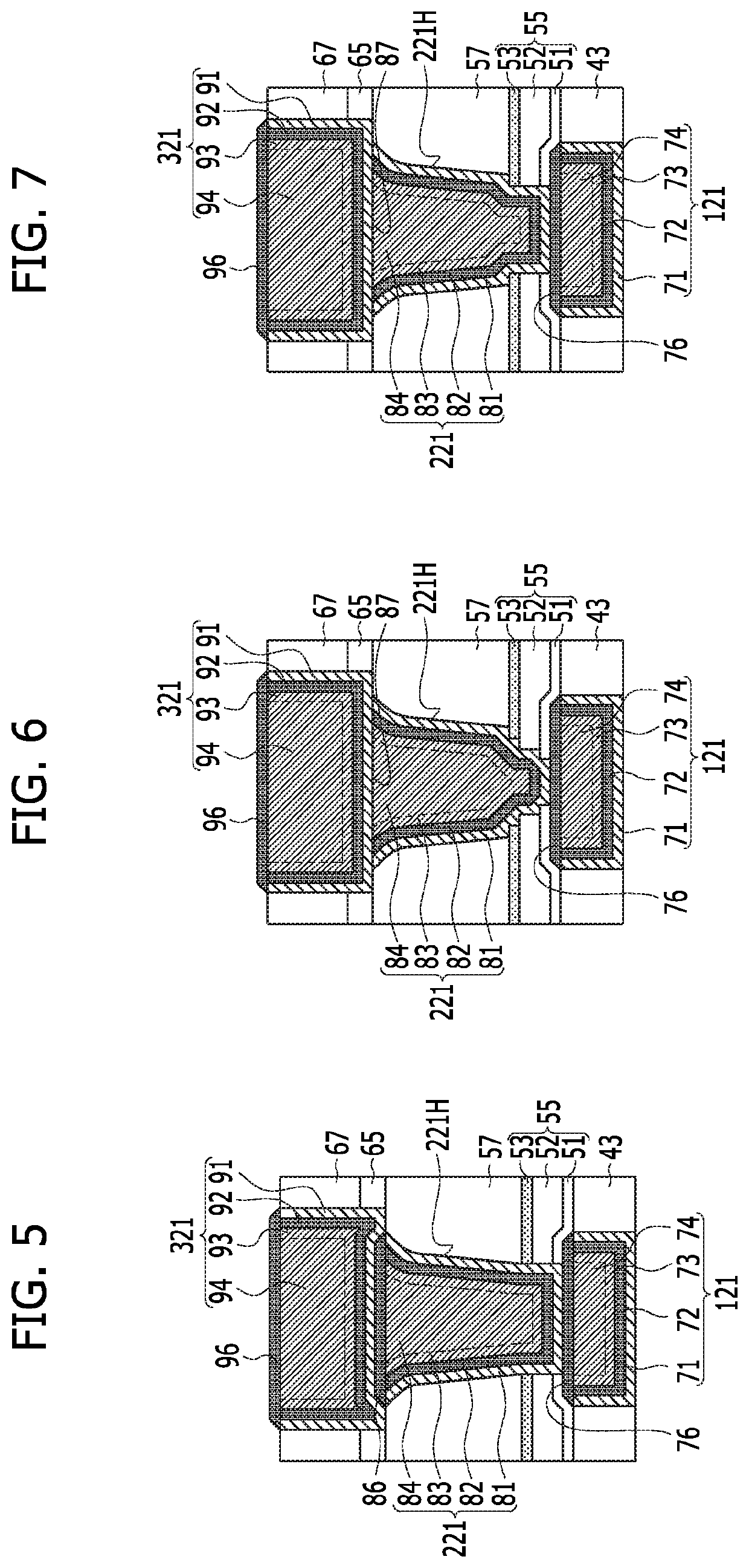
[0020]A process of forming contact plugs using a single damascene process may cause various defects during a chemical mechanical polishing (CMP) process due, for example, to the density, gaps, and / or shapes of contact holes / plugs. In order to achieve more uniform density and gaps of the contact plugs on an entire substrate, dummy contact plugs may be around main contact plugs. Arrangement of the main contact plugs and the dummy contact plugs may be directly affected by upper and lower interconnections.

[0021]The main contact plug may serve to exchange signals between the upper interconnection and the lower interconnection. A wide contact area of the upper interconnection and the contact plug may be advantageous for transmission of a signal. Expanding an upper region of the contact hole for reducing contact resistance between the contact plug and the upper interconnection may be advantageous. A structure capable of minimizing or reducing a leakage current may be advantageous for a con...


PUM

PropertyMeasurementUnit
widthaaaaaaaaaa
areaaaaaaaaaaa
conductiveaaaaaaaaaa

Abstract

A semiconductor device includes a plurality of main contact plugs and a plurality of dummy contact plugs which pass through an insulating layer on a substrate. A plurality of upper interconnections is on the insulating layer. The plurality of dummy contact plugs include a first dummy contact plug. The plurality of upper interconnections include a first upper interconnection overlapping the first dummy contact plug. A vertical central axis of the first dummy contact plug is located outside the first upper interconnection.

Description

CROSS-REFERENCE TO RELATED APPLICATION[0001]This U.S. non-provisional patent application claims priority under 35 U.S.C. § 119 to and the benefit of Korean Patent Application No. 10-2017-0102492, filed on Aug. 11, 2017, in the Korean intellectual Property Office (KIPO), the disclosure of which is incorporated herein by reference in its entirety.BACKGROUND[0002]Inventive concepts relate to a semiconductor device including a dummy contact plug.[0003]A process of forming contact plugs and interconnections is becoming increasingly difficult, for example owing to high integration of semiconductor devices. A single damascene process has been attempted to form the contact plugs. The single damascene process may generate various defects, such as dishing, due to the arrangement of the contact plugs. A new technique is desired to optimize or improve the arrangement of the contact plugs.SUMMARY OF THE INVENTION[0004]Inventive concepts are directed to providing a semiconductor device which is a...

Claims


Application Information

Patent Timeline
Patent Type & Authority Patents(United States)
IPC IPC(8): H01L23/528H01L23/522H01L21/768H01L21/311H01L23/532H01L21/285
CPCH01L23/5283H01L21/31122H01L21/7684H01L21/76804H01L21/76805H01L21/76816H01L21/76832H01L23/5226H01L21/28568H01L21/76846H01L21/76852H01L23/53238H01L23/53295H01L23/522H01L21/76834H01L21/76849H01L21/76897H01L21/76841H01L21/76829
Inventor OH, IN WOOKKIM, DONG HYUNPARK, DOO HWANPARK, SUNG KEUNPARK, CHUL HONGHWANG, SUNG WOOK
Owner SAMSUNG ELECTRONICS CO LTD
Learn More