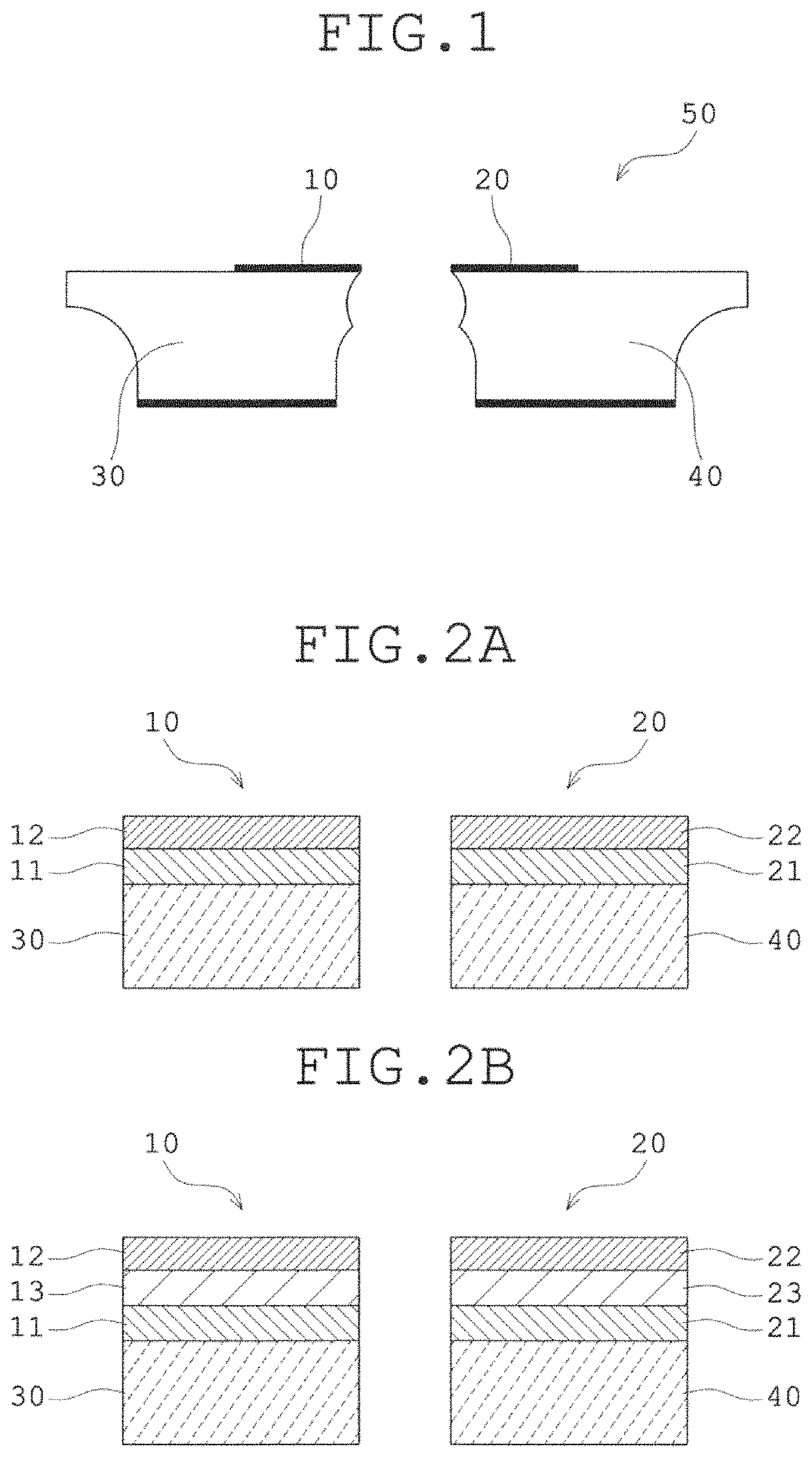
Lead frame, resin-equipped lead frame, optical semiconductor device, and method for manufacturing lead frame
a technology of lead frame and resin, which is applied in the direction of semiconductor devices, semiconductor/solid-state device details, electrical devices, etc., can solve the problems of deteriorating the productivity reducing the product quality of lead frame products, and reducing the cost of noble metals used to increase the gloss of coating surfaces. , to achieve the effect of preventing appearance defects and cost reduction
- Summary
- Abstract
- Description
- Claims
- Application Information
AI Technical Summary
Benefits of technology
Problems solved by technology
Method used
Image
Examples
embodied examples
[0181]Next, a lead frame, a resin-equipped lead frame, and an optical semiconductor device according to one embodiment of the present invention will be described in detail in reference to Embodied Examples. It is noted that the present invention is not limited to these Embodied Examples.
embodied example 1
[0182]A lead frame for an optical semiconductor device of Embodied Example 1 was fabricated by means of post-plating method in which, after formation of a lead frame pattern, full plating was performed over the entire surface of the pattern.
[0183]To be specific, first, as a metal plate for forming a lead frame, a Cu plate having a thickness of 0.2 mm was processed into a long plate having a width of 140 mm, and then a photosensitive dry film resist having a thickness of 0.05 mm was applied to the both sides of the metal plate with a laminating roll.
[0184]Then, the dry film resist, on the front and back sides, was covered with a glass mask that carried a predetermined pattern for forming a die pad portion and a lead portion and was exposed to ultraviolet light. Thereafter, using a sodium carbonate solution, development treatment was performed to dissolve uncured dry film resist that failed to be irradiated with ultraviolet light and was left unaffected.
[0185]Then, exposed faces of th...
embodied example 2 to embodied example 7
[0190]In Embodied Example 2, a lead frame, a resin-equipped lead frame, and an optical semiconductor device were fabricated in the same manner as in Embodied Example 1 except that the thickness of the glossy Ni plating layer was 0.5 μm.
[0191]In Embodied Example 3, a lead frame, a resin-equipped lead frame, and an optical semiconductor device were fabricated in the same manner as in Embodied Example 1 except that the thickness of the glossy Ni plating layer was 3.0 μm.
[0192]In Embodied Example 4, a lead frame, a resin-equipped lead frame, and an optical semiconductor device were fabricated in the same manner as in Embodied Example 1, except that adjustment was made so that a surface roughness in terms of Ra of the glossy Ni plating layer be 0.02 μm, the gloss of the glossy Ni coating surface be 3.1, and the gloss at the Ag coating surface be 2.1.
[0193]In Embodied Example 5, a lead frame, a resin-equipped lead frame, and an optical semiconductor device were fabricated in the same mann...
PUM
| Property | Measurement | Unit |
|---|---|---|
| Ra | aaaaa | aaaaa |
| thickness | aaaaa | aaaaa |
| thickness | aaaaa | aaaaa |
Abstract
Description
Claims
Application Information
 - R&D
- Intellectual Property
- Life Sciences
- Materials
- Tech Scout
- Unparalleled Data Quality
- Higher Quality Content
- 60% Fewer Hallucinations
Browse by: Latest US Patents, China's latest patents, Technical Efficacy Thesaurus, Application Domain, Technology Topic, Popular Technical Reports.
© 2025 PatSnap. All rights reserved.Legal|Privacy policy|Modern Slavery Act Transparency Statement|Sitemap|About US| Contact US: help@patsnap.com


