Eureka AIR delivers breakthrough ideas for toughest innovation challenges, trusted by R&D personnel around the world.

Pattern forming method as well as production methods for processed substrate, optical component, circuit board, electronic component and imprint mold

a technology of substrate and forming method, applied in the direction of instruments, photomechanical devices, other domestic objects, etc., can solve the problem of low throughput and achieve the effect of improving throughput and excellent uniformity

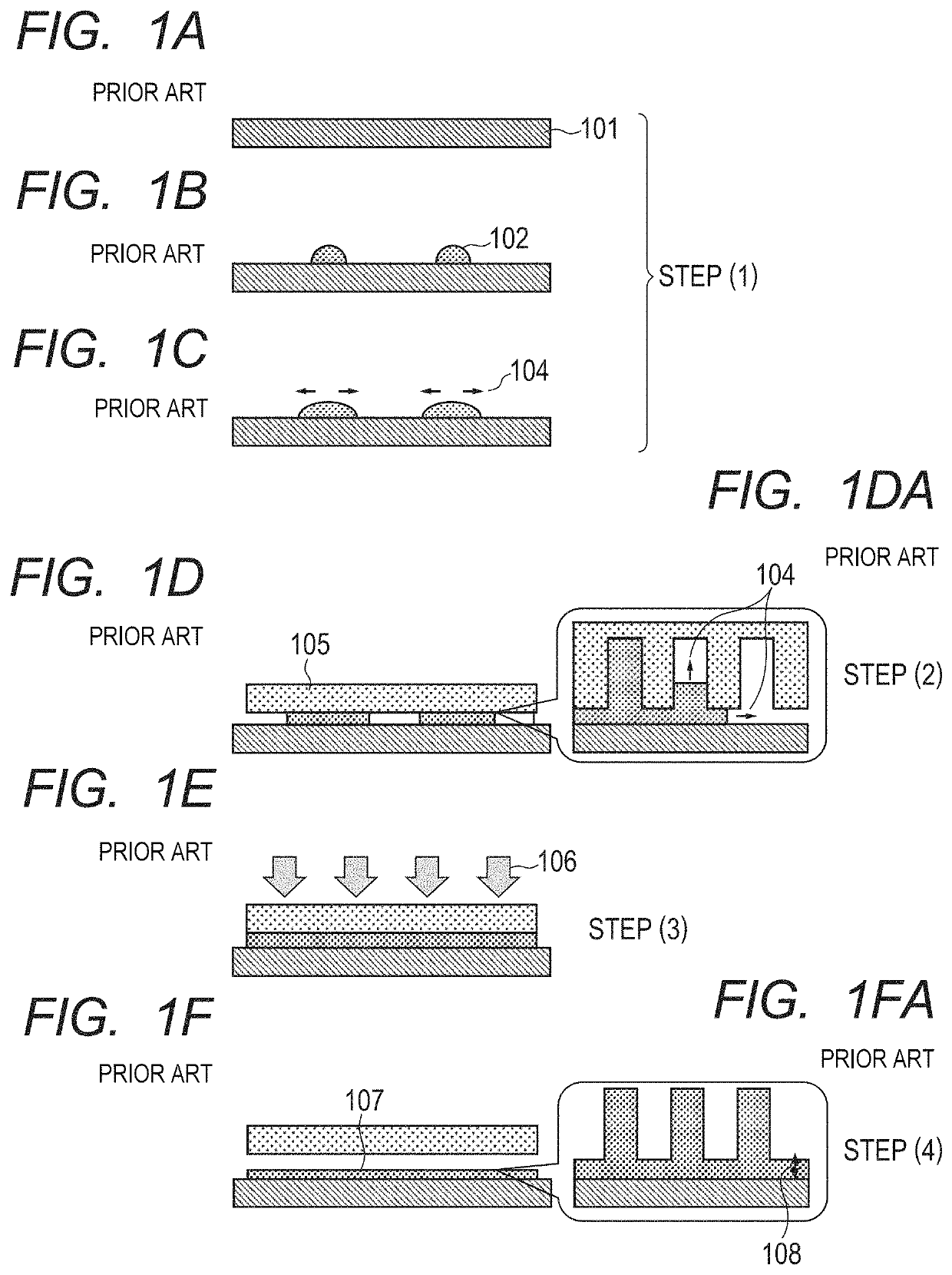
Active Publication Date: 2020-08-25
CANON KK
View PDF55 Cites 4 Cited by
  • Summary
  • Abstract
  • Description
  • Claims
  • Application Information

AI Technical Summary

Benefits of technology

[0018]An object of the present invention is to provide a SST-NIL technology which is improved in throughput and by which a uniform pattern can be formed on a substrate.
[0028]According to the present invention, there can be provided the pattern forming method improved in throughput and excellent in uniformity.

Problems solved by technology

The photo-nanoimprint technology disclosed in Japanese Patent No. 4791357 has involved a problem in that a time period (filling time) from the initiation of the contact of the mold to the completion of the spread and the fill is long, and hence throughput is low.

Method used


Image

  • Pattern forming method as well as production methods for processed substrate, optical component, circuit board, electronic component and imprint mold
  • Pattern forming method as well as production methods for processed substrate, optical component, circuit board, electronic component and imprint mold
  • Pattern forming method as well as production methods for processed substrate, optical component, circuit board, electronic component and imprint mold

Examples


example 1

[0179](1) Preparation of Curable Composition (A1-1)

[0180]A component (a1), a component (b1), a component (c1), and a component (d1) described below were blended, and the blend was filtered with a 0.2-micrometer filter made of ultrahigh-molecular weight polyethylene to prepare a curable composition (A1-1) of Example 1.

[0181]

(1-1) Component (a1):100parts by weight in totalTrimethylolpropane triacrylate100parts by weight(manufactured by Sigma-Aldrich,abbreviation: TMPTA):(1-2) Component (b1):0parts by weight in total

[0182]The component (b1) was not added.

[0183]

(1-3) Component (c1)0 parts by weight in total

[0184]The component (c1) was not added.

[0185]

(1-4) Component (d1):33,000parts by weight in totalPropylene glycol monomethyl ether33,000parts by weightacetate (manufactured by TokyoChemical Industry Co., Ltd.,abbreviation: PGMEA):

[0186](2) Preparation of Curable Composition (A2-1)

[0187]A component (a2), a component (b2), a component (c2), and a component (d2) described below were blend...

example 2

[0197](1) to (3) Curable Compositions (A1) and (A2)

[0198]The same compositions as that of Example 1 were used as a curable composition (A1) and (A2).

[0199](4) Discussion on Prespread Promoting Effect

[0200]It is hypothesized that the residual ratio of the component (d1) serving as a solvent in the film of the curable composition (A1-1) is 10 wt %. The surface tension of the film of the curable composition (A1-1) is 35.1 mN / m, and is higher than the surface tension of the curable composition (A2-1), i.e., 32.7 mN / m by 2 mN / m or more. Accordingly, a strong prespread promoting effect can be obtained.

[0201](5) Discussion on Pattern Formation Uniformity in Shot Region

[0202]Similarly, it is hypothesized that the residual ratio of the component (d1) serving as a solvent in the film of the curable composition (A1-1) is 10 wt %. The volatility of the component (a1) is low and an influence of the volatilization of the component (d1) serving as a solvent is slight. Accordingly, the Marangoni ef...


PUM

PropertyMeasurementUnit
viscosityaaaaaaaaaa
viscosityaaaaaaaaaa
wt %aaaaaaaaaa

Abstract

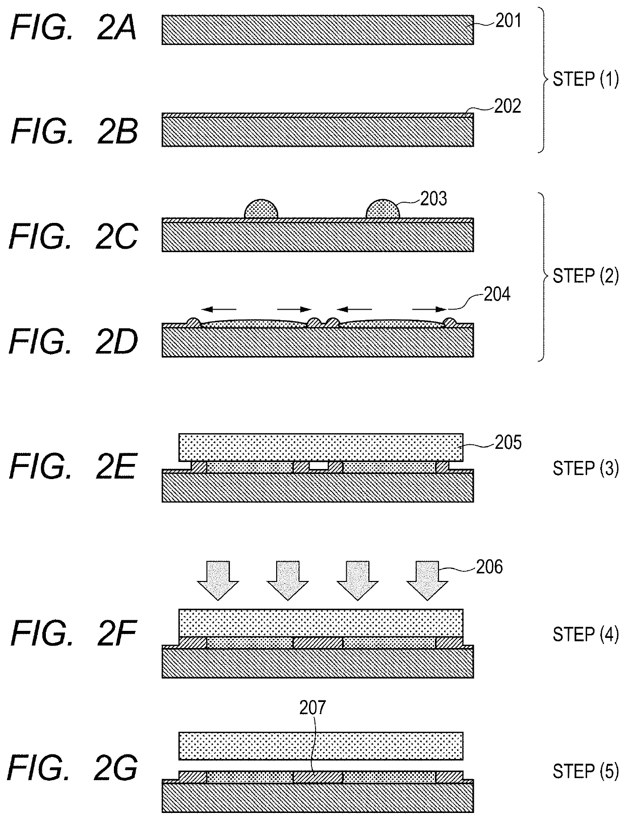
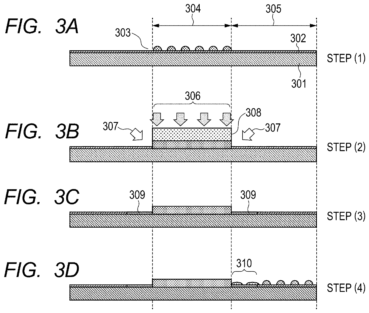
A pattern is formed on a substrate with forming a layer of a curable composition (A1) containing a component (a1) serving as a polymerizable compound and a component (d1) serving as a solvent on a surface of the substrate, then dispensing droplets of a curable composition (A2) containing at least a component (a2) serving as a polymerizable compound dropwise discretely onto the layer of the curable composition, subsequently sandwiching a mixture layer of the curable composition (A1) and the curable composition (A2) between a mold and the substrate, then irradiating the mixture layer with light to cure the layer, and releasing the mold from the mixture layer after the curing.

Description

BACKGROUND OF THE INVENTIONField of the Invention[0001]The present invention relates to a pattern forming method, a method of producing a processed substrate, a method of producing an optical component, a method of producing a circuit board, a method of producing an electronic component, and a method of producing an imprint mold.Description of the Related Art[0002]There has been a growing requirement for miniaturization in a semiconductor device, a MEMS, or the like, and hence a photo-nanoimprint technology has been attracting attention as a microfabrication technology.[0003]In the photo-nanoimprint technology, a photocurable composition (resist) is cured in a state in which a mold having a fine groove / land pattern formed on its surface is pressed against a substrate (wafer) having applied thereto the photocurable composition. Thus, the groove / land pattern of the mold is transferred onto the cured film of the photocurable composition and hence the pattern is formed on the substrate....

Claims


Application Information

Patent Timeline
Patent Type & Authority Patents(United States)
IPC IPC(8): G03F7/00C09D135/02C09D133/06
CPCC09D133/06C09D135/02G03F7/0002B05D1/30B05D3/04B05D3/12B29C59/026G03F7/161B29L2011/00B29L2031/34
Inventor ITO, TOSHIKIOTANI, TOMONORICHIBA, KEIKOLIU, WEIJUNSTACHOWIAK, TIMOTHY BRIAN
Owner CANON KK
Why Eureka
Eureka Blog
Learn More