Optically activated transistor, switch, and photodiode

a technology of optically activated transistors and switch bodies, applied in semiconductor devices, vacuum evaporation coatings, coatings, etc., can solve the problems of non-appreciable current for typical transistors and fets that may not be usable in some applications, and achieve the effect of increasing curren

Active Publication Date: 2020-06-30
BOISE STATE UNIVERSITY
View PDF26 Cites 0 Cited by
  • Summary
  • Abstract
  • Description
  • Claims
  • Application Information

AI Technical Summary

Problems solved by technology

Because a FET relies on a voltage applied to a gate terminal for its operation, a FET may not be usable in some applications where a gate signal takes a form other than voltage.
The active material conducts current in the presence of light, but only conducts a very small amount of current in the absence of light, the current being non-appreciable for typical transistor, switch, and diode applications.

Method used


Image

  • Optically activated transistor, switch, and photodiode
  • Optically activated transistor, switch, and photodiode
  • Optically activated transistor, switch, and photodiode

Examples


Embodiment Construction

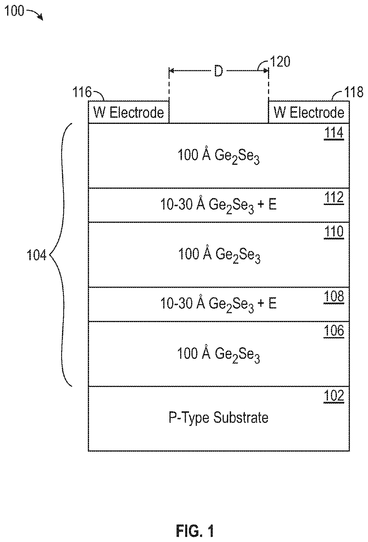
[0023]FIG. 1 shows a block diagram of an optically activated device 100. The device 100 may include active material 104 deposited onto a substrate 102. The substrate may include doped silicon. In particular, the substrate may include a p-type silicon substrate. While an n-type substrate may also be contemplated, a p-type silicon substrate was shown to exhibit transistor properties as described herein.

[0024]The p-type silicon substrate may further include a native oxide layer (not shown). While other coatings of the p-type silicon substrate are also contemplated, the native oxide layer was shown to exhibit desirable transistor properties. In some embodiments, the substrate may be flexible. Other substrates are also contemplated as would be appreciated by one of ordinary skill in the art having the benefit of this disclosure.

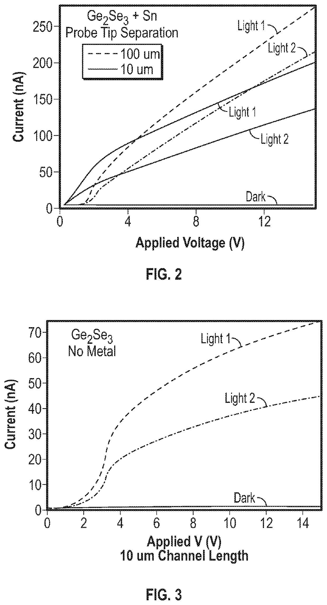
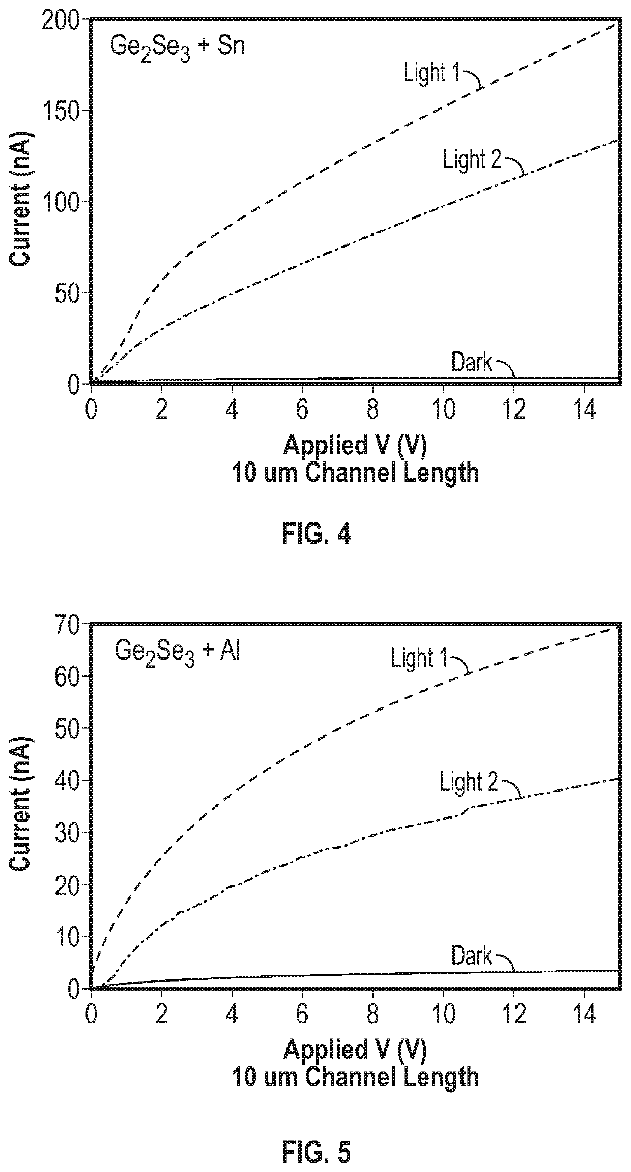
[0025]The active material 104 may include various layers 106, 108, 110, 112, 114. The first layer 106 may include GeSe alone without the addition of other element...


PUM

PropertyMeasurementUnit
thicknessaaaaaaaaaa
thicknessaaaaaaaaaa
thicknessaaaaaaaaaa

Abstract

An optically activated device that includes an active material on a substrate with two electrodes electrically connected to the active material, the active material conducts current in the presence of light and does not conduct appreciable current in the absence of light. The optically activated device functions as a photodiode, a switch, and an optically gated transistor. The optically activated device conducts current in the presences of light. The active material may be layers of germanium selenide and germanium selenide and an element. Germanium selenide may be sputtered onto a substrate to create layers of material separated by layers of co-sputtered germanium selenide with the element. The active material may be deposited onto a flexible substrate.

Description

CROSS-REFERENCE TO RELATED APPLICATIONS[0001]This application claims priority to and the benefit of U.S. Provisional Patent Application Ser. No. 62 / 511,119 filed on May 25, 2017, and entitled “Optically Activated Transistor, Switch, and Photodiode,” the contents of which are hereby incorporated by reference herein in their entirety.GOVERNMENT LICENSE RIGHTS[0002]The invention disclosed herein was funded in-part or in-whole by the U.S. Air Force Research Laboratory under Contract No. FA8750-16-C-0183. The government has certain rights in the invention disclosed herein.BACKGROUNDField of the Disclosure[0003]The embodiments described herein relate to apparatuses that conduct current bi-directionally in the presence of light, methods of conducting current bi-directionally in the presence of light, and methods of providing such apparatuses.Description of the Related Art[0004]A photodiode is a device that generates current in the presence of light. The photodiode generates the electrical ...

Claims


Application Information

Patent Timeline
Patent Type & Authority Patents(United States)
IPC IPC(8): H01L31/043H01L31/0224H01L31/032C23C14/06C23C14/34H01L31/109
CPCH01L31/0324C23C14/0623H01L31/032H01L31/022408C23C14/34H01L31/109C23C14/0629C23C14/14C23C14/3464
Inventor CAMPBELL, KRISTY A.
Owner BOISE STATE UNIVERSITY
Why Eureka
Try Eureka