Atomic cell, atomic cell manufacturing method, quantum interference device, atomic oscillator, electronic apparatus, and vehicle
a quantum interference and manufacturing method technology, applied in the direction of pre-selected time interval producing apparatus, automatic control, instruments, etc., can solve the problems of low melting point and heat resistance of paraffin, and achieve excellent reliability
- Summary
- Abstract
- Description
- Claims
- Application Information
AI Technical Summary
Benefits of technology
Problems solved by technology
Method used
Image
Examples
first embodiment
1. First Embodiment
1.1. Atomic Cell
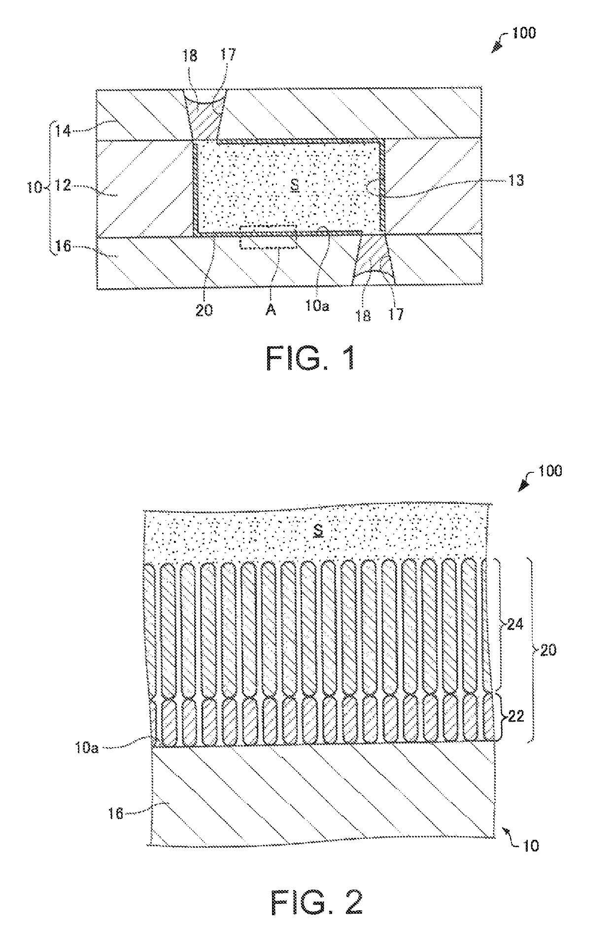
[0064]First, an atomic cell according to a first embodiment will be described with reference to the drawings. FIG. 1 is a cross-sectional view schematically showing an atomic cell 100 according to the first embodiment. FIG. 2 is a cross-sectional view schematically showing the atomic cell 100 according to the first embodiment, and is an enlarged view of a region A shown in FIG. 1. FIG. 3 is a perspective view schematically showing the atomic cell 100 according to the first embodiment.
[0065]As shown in FIGS. 1 to 3, the atomic cell 100 includes a substrate 10 and a coating layer 20. The coating layer 20 includes a first coating layer 22 and a second coating layer 24. The atomic cell 100 is used in, for example, an atomic oscillator.
[0066]The substrate 10 includes a trunk 12, and a pair of windows 14 and 16 provided so as to interpose the trunk 12 therebetween. In the trunk 12, a cylindrical through-hole 13 is formed. By the through-hole 13, an inter...
second embodiment
2. Second Embodiment
2.1. Atomic Cell
[0098]Next, an atomic cell according to a second embodiment will be described with reference to the drawings. FIG. 10 is a cross-sectional view schematically showing an atomic cell 110 according to this embodiment. Hereinafter, in the atomic cell 110 according to the second embodiment, members having the same functions as those of the constituent members of the atomic cell 100 according to the above-mentioned first embodiment are denoted by the same reference numerals, and the detailed description thereof will be omitted.
[0099]As shown in FIG. 10, the atomic cell 110 is different from the above-mentioned atomic cell 100 in that the coating layer 20 includes a first coating layer 122, a second coating layer 124, and a third coating layer 126.
[0100]The windows 14 and 16 are formed from a material containing a compound having a polar group as described above. Specifically, the windows 14 and 16 are formed from a material such as quartz glass or boros...
third embodiment
3. Third Embodiment
[0128]Next, an atomic oscillator (quantum interference device) according to a third embodiment will be described with reference to the drawings. The quantum interference device according to the embodiment includes the atomic cell according to the embodiments. Hereinafter, an atomic oscillator including the atomic cell 100 according to the embodiment will be described. The quantum interference device according to the embodiment can also be applied to, for example, a magnetic sensor, a quantum memory, or the like other than the atomic oscillator.
[0129]FIG. 15 is a functional block diagram of an atomic oscillator 200 according to the third embodiment. FIG. 16 is a view for illustrating the energy state of an alkali metal in the atomic cell 100 of the atomic oscillator 200 according to the third embodiment. FIG. 17 is a graph showing a relationship between a difference in frequency between two lights emitted from a light emitter and a detection intensity detected by a...
PUM
 Abstract
Description
Claims
Application Information
 - R&D Engineer
- R&D Manager
- IP Professional
- Industry Leading Data Capabilities
- Powerful AI technology
- Patent DNA Extraction
Browse by: Latest US Patents, China's latest patents, Technical Efficacy Thesaurus, Application Domain, Technology Topic, Popular Technical Reports.
© 2024 PatSnap. All rights reserved.Legal|Privacy policy|Modern Slavery Act Transparency Statement|Sitemap|About US| Contact US: help@patsnap.com


