
Single-layer circuit board, multi-layer circuit board, and manufacturing methods therefor

a single-layer circuit board and manufacturing method technology, applied in the direction of printed element electric connection formation, catalyst application resist, vacuum evaporation coating, etc., can solve the problems of copper layer easily peeling off from the hole wall, weak binding force between electroplating copper layer and hole wall, and deviation of drilling position on the substrate, etc., to improve the conductive performance of metalized holes and simplify circuit board manufacturing procedures

Active Publication Date: 2019-06-11
RICHVIEW ELECTRONICS CO LTD
View PDF14 Cites 3 Cited by
  • Summary
  • Abstract
  • Description
  • Claims
  • Application Information

AI Technical Summary

Benefits of technology

[0008]the invention is made in view of above-mentioned problems, the aim is to, provide single-layer circuit board with metalized hole, multi-layer circuit board and manufacturing methods thereof, to simplify the manufacturing procedure of circuit board, and improve conductive performance of metalized hole therein.

Problems solved by technology

However, in the etching thinning process, once etching position generates deviation, it will result in that drilling position on the substrate also generates deviation.
Also, when implementing metalization to mini-hole, binding force between electroplating copper layer and hole wall is weak, copper layer easily peels off from the hole wall.
Additionally, the minimal diameter of micro-hole manufactured on the overlaying copper plate utilizing prior art is 20-50 μm, when the diameter is less than 20 μm, it will generate a hole with too high thickness-diameter ratio and problems of hole wall copper layer being nonuniform or the like will occur at the time of electroless copper and electroplating.
Therefore, void or crack easily forms in the deposition process, it will also result in that the copper thickness of hole surface is larger than the copper thickness of hole wall.
Additionally, above-mentioned methods of producing circuit board need to produce finished overlaying copper plate in advance, afterward implementing drilling and hole metalization to the finished overlaying copper plate, then make circuit pattern via procedure of pasting film, exposure and development, etching or the like, thus the process procedure is long, the producing cost is high.
Also, because there are several metal etching in the whole process procedure, thus it will generate plenty of waste water containing metal ion, generating significant harm to environment.

Method used


Image

  • Single-layer circuit board, multi-layer circuit board, and manufacturing methods therefor
  • Single-layer circuit board, multi-layer circuit board, and manufacturing methods therefor
  • Single-layer circuit board, multi-layer circuit board, and manufacturing methods therefor

Examples


example 1

[0137]Such example uses organic polymer thin film as substrate to make flexible circuit board having metalized hole, particularly utilizing liquid crystal polymer thin film (LCP film) as substrate.

[0138]First, the surface of LCP film is rubbed using gauze impregnated by alcohol, to remove the dirt adhered above. Subsequently, a series of through holes with the diameter of 20 μm are drilled on such LCP film utilizing laser drilling technology, then the surface of LCP film and the hole wall are thoroughly cleaned using blower or the like, to remove drilling scrap and other dirt left therein.

[0139]Then, one layer of photoresist film is painted on the cleaned LCP film substrate surface, and such substrate is placed on a lithography machine to implement exposure and development, afterward material in the region is washed away to form circuit pattern on the substrate surface (also known as circuit region), circuit negative image overlaid with photoresist film coating (also known as photor...

example 2

[0144]Such example uses epoxy glass fabric as substrate to manufacture rigid single-layer circuit board having metalized hole, in turn uses such single-layer circuit board to make multi-layer circuit board, particularly using FR-4 or FR-5 substrate of the epoxy glass fabric substrate.

[0145]First, the surface of FR-4 substrate is rubbed using gauze impregnated by alcohol; to remove the dirt adhered above. Subsequently, several through holes with the diameter of about 100 μm and several blind holes with the diameter of about 100 μm and in a depth of about 200 μm are drilled on such FR-4 substrate utilizing laser drilling technology. After drilling the holes, the surface of FR-4 substrate and the hole wall are further thoroughly washed using ultrasonic technology and baking treatment is implemented, to remove drilling scrap and other dirt left therein.

[0146]Subsequently, the substrate after baking is placed into an ion implantation equipment via feeding mechanism, the ion implantation ...

example 3

[0156]This example uses double-face flexible overlaying copper plate with organic polymer thin film (for example, PI film) as substrate to make single-layer circuit board, further uses such single-layer circuit board to make multi-layer circuit board.

[0157]First, single-layer circuit board is prepared. In particular, PI film is used as substrate, two surfaces of PI film are rubbed using gauze impregnated by alcohol, to remove the dirt adhered above. Subsequently, a series of through holes with the diameter of 10 μm on PI film are drilled utilizing ultraviolet laser drilling technology, and the surface and the hole wall of PI film are thoroughly washed using ultrasonic technology, to remove drilling scrap and other dirt left therein. Subsequently, PI film after drilling is placed into ion implantation equipment. In such ion implantation equipment, the ion implantation chamber is vacuumed to 1×10⁻⁴Pa, Ni is used as target material, proper implanting voltage, implanting current is sele...


PUM

PropertyMeasurementUnit
thicknessaaaaaaaaaa
depthaaaaaaaaaa
diameteraaaaaaaaaa

Abstract

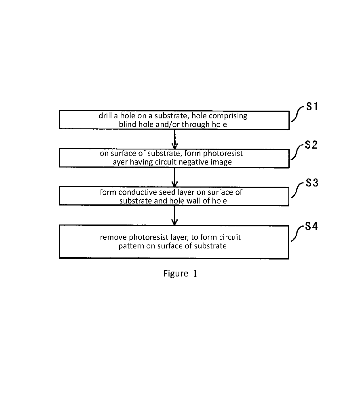
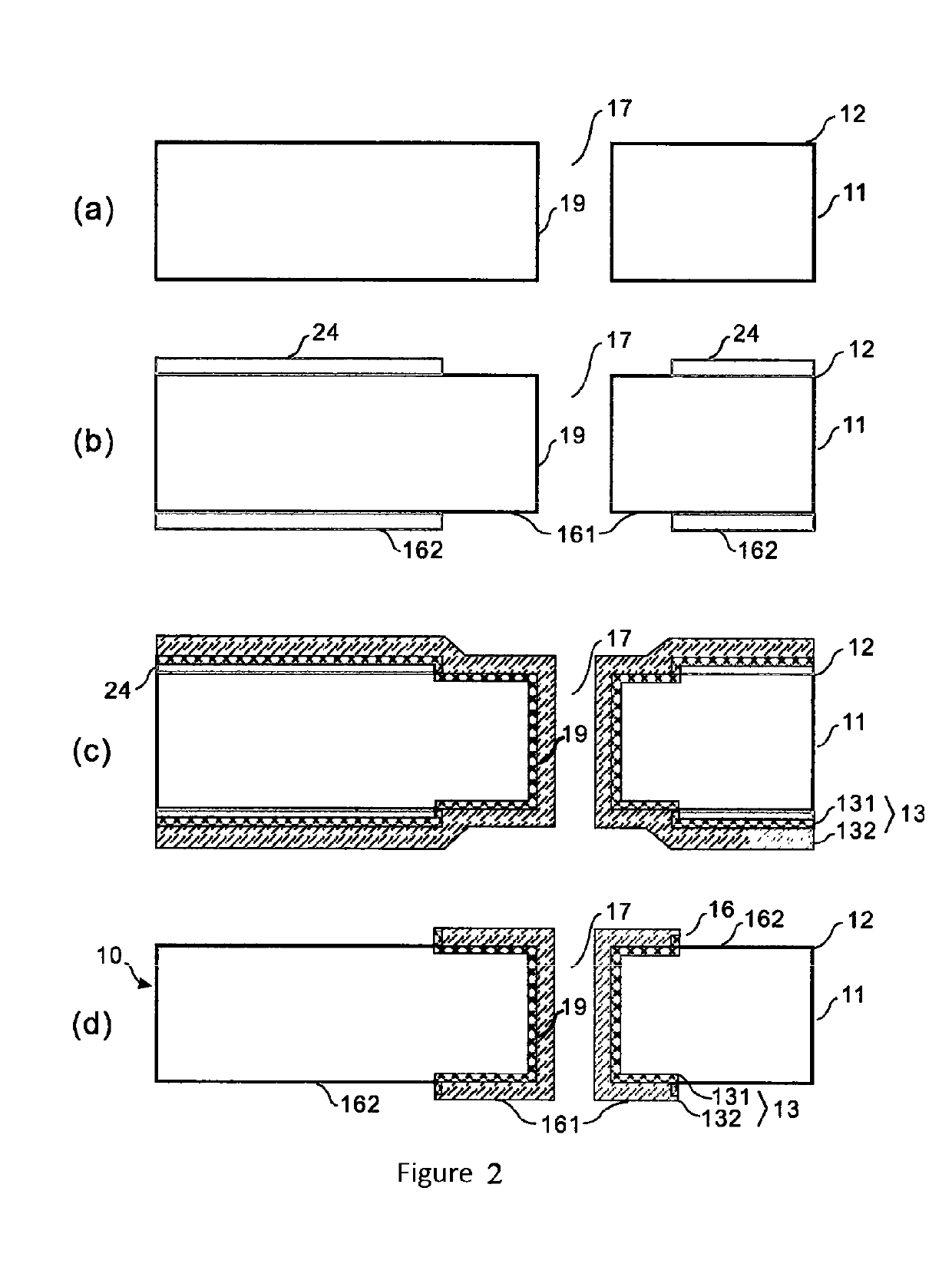
A single-layer circuit board, multi-layer circuit board, and manufacturing methods therefor. The method for manufacturing the single-layer circuit board (10) comprises the following steps: drilling a hole on a substrate (11), the hole comprising a blind hole and / or a through hole (S1); on a surface (12) of the substrate, forming a photoresist layer having a circuit negative image (S2); forming a conductive seed layer on the surface (12) of the substrate and a hole wall (19) of the hole (S3); removing the photoresist layer, and forming a circuit pattern on the surface (12) of the substrate (S4), wherein Step S3 comprises implanting a conductive material below the surface (12) of the substrate and below the hole wall (19) of the hole via ion implantation, and forming an ion implantation layer as at least part of the conductive seed layer.

Description

CROSS-REFERENCE TO RELATED APPLICATIONS[0001]This application is a U.S. national stage application under 35 U.S.C § 371 of PCT / CN2016 / 000649, filed on Nov. 23, 2016, which claims the benefit of and priority to Chinese Patent Application No. 201510747884.1, filed Nov. 6, 2015, the contents of which are herein incorporated by reference in their entirety.FIELD[0002]the invention relates to single-layer circuit board, multi-layer circuit board and manufacturing methods thereof. Especially, the invention relates to single-layer circuit board with insulated material having a hole as substrate and formed with conductor layer on the hole wall and formed with circuit pattern on the substrate surface, multi-layer circuit board laminated by plenty of single-layer circuit boards and wherein each single-layer circuit board is connected via metalized via hole, and manufacturing methods thereof.BACKGROUND[0003]In the circuit board industry, metalized via hole is widely used to connect surface of c...

Claims


Application Information

Patent Timeline
Patent Type & Authority Patents(United States)
IPC IPC(8): H05K1/02H05K3/42C23C14/48H05K1/11
CPCH05K3/429C23C14/48H05K3/42H05K1/115H05K2203/092H05K2201/096H05K3/048H05K3/06H05K3/105H05K3/108H05K3/421H05K3/422H05K3/423H05K3/426H05K3/427H05K3/4617H05K2201/0355H05K2203/0565H05K2203/0769H05K2203/1423
Inventor BAI, SIPINGWU, XIANGLANWANG, ZHIJIANYANG, ZHIGANGZHANG, JINQIANG
Owner RICHVIEW ELECTRONICS CO LTD
Learn More