Semiconductor device, electronic component, and electronic device
a technology of semiconductor devices and electronic components, applied in pulse generators, pulse techniques, instruments, etc., can solve the problems of difficult to ensure a long data retention time, easy leakage of accumulated charge, and increase of leakage current flowing between a gate and a semiconductor layer, so as to achieve faster operation, lower power consumption, and high integration of a semiconductor device
- Summary
- Abstract
- Description
- Claims
- Application Information
AI Technical Summary
Benefits of technology
Problems solved by technology
Method used
Image
Examples
embodiment 1
[0048]This embodiment will explain an example of a semiconductor device that has a function of a nonvolatile memory device applicable to a register or the like.
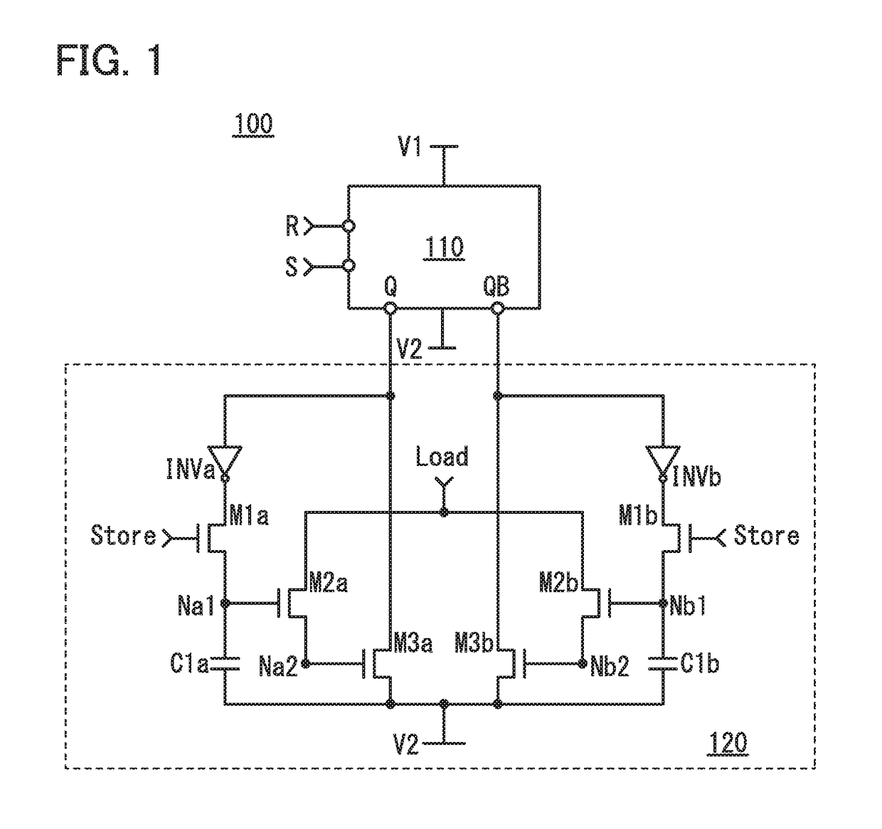
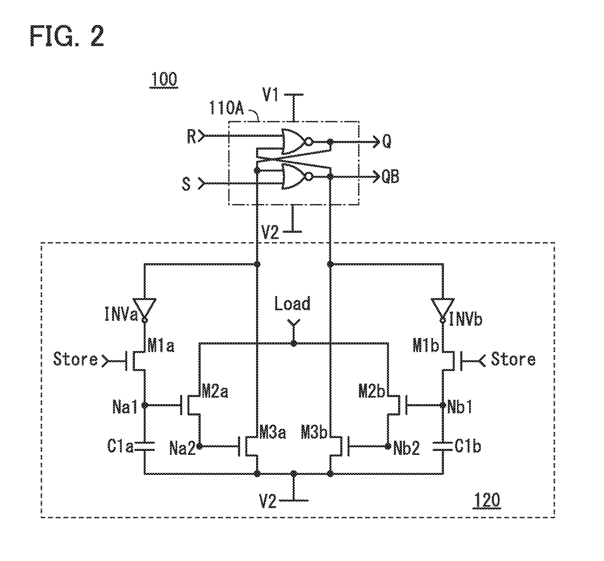
[0049]FIG. 1 is a circuit diagram illustrating an example of a circuit configuration of a semiconductor device 100. The semiconductor device 100 includes a circuit 110 and a circuit 120.
[0050]The circuit 110 has a function of storing data while power supply voltage is supplied. The circuit 120 has a function of storing data even while power supply voltage is not supplied.
[0051]The circuit 110 is a latch, for example. In FIG. 1, the circuit 110 is an SR latch having an input terminal R, an input terminal S, an output terminal Q, and an output terminal QB.
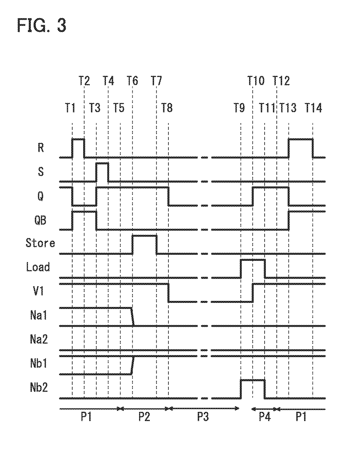
[0052]The circuit 120 is composed of a combination of a transistor containing an oxide semiconductor in its channel formation region (OS transistor) and a transistor containing silicon in its channel formation region (Si transistor), and stores data by holding charge correspon...
embodiment 2
[0085]This embodiment will explain the OS transistor described in the foregoing embodiment.
[0086]The off-state current of an OS transistor can be reduced by reducing the concentration of impurities in an oxide semiconductor to make the oxide semiconductor intrinsic or substantially intrinsic. The term “substantially intrinsic” refers to a state where an oxide semiconductor has a carrier density lower than 8×10¹¹ / cm3, preferably lower than 1×10¹¹ / cm3, more preferably lower than 1×10¹⁰ / cm3, and is higher than or equal to 1×10⁻⁹ / cm3. In the oxide semiconductor, hydrogen, nitrogen, carbon, silicon, and a metal element other than main components of the oxide semiconductor are impurities. For example, hydrogen and nitrogen form donor levels to increase the carrier density.
[0087]A transistor using an intrinsic or substantially intrinsic oxide semiconductor has a low carrier density and thus is less likely to have negative threshold voltage. In addition, because of few carrier traps in such...
embodiment 3
[0148]In this embodiment, a cross-sectional structure of a transistor included in a semiconductor device of one embodiment of the disclosed invention will be described with reference to drawings.
[0149]First, schematic views of a cross-sectional structure of the semiconductor device of one embodiment of the present invention will be described with reference to FIGS. 11A and 11B.
[0150]Transistors included in the semiconductor device of one embodiment of the present invention are Si transistors and OS transistors. For example, the semiconductor device has a cross-sectional structure in which a layer including Si transistors and a layer including OS transistors are stacked. Each of the layers includes a plurality of transistors including a semiconductor layer of the same material.
[0151]For example as illustrated in FIG. 11A, the semiconductor device of one embodiment of the present invention can be formed by stacking a layer 31 including Si transistors (represented as Si-FET Layer in FI...
PUM
 Abstract
Description
Claims
Application Information
 - R&D Engineer
- R&D Manager
- IP Professional
- Industry Leading Data Capabilities
- Powerful AI technology
- Patent DNA Extraction
Browse by: Latest US Patents, China's latest patents, Technical Efficacy Thesaurus, Application Domain, Technology Topic, Popular Technical Reports.
© 2024 PatSnap. All rights reserved.Legal|Privacy policy|Modern Slavery Act Transparency Statement|Sitemap|About US| Contact US: help@patsnap.com


