
Scanning imaging system with a novel imaging sensor with gaps for electronic circuitry

a scanning imaging and electronic circuit technology, applied in the field of sample detection, can solve the problems of reducing the relative low speed of reading out the region, and achieve the effects of improving image quality, increasing the fill factor of the pixel, and increasing the low light sensitivity of the imaging sensor

Active Publication Date: 2018-10-02
KONINKLJIJKE PHILIPS NV
View PDF15 Cites 0 Cited by
  • Summary
  • Abstract
  • Description
  • Claims
  • Application Information

AI Technical Summary

Benefits of technology

This configuration enhances low light sensitivity and image quality while enabling faster image generation by maximizing the photoactive area and reducing noise, particularly in tilted sensor configurations.

Problems solved by technology

However, such non-photosensitive parts of the pixel reduce the fill factor of the pixel which is especially harming during low light conditions.
In addition, currently available imaging sensors provide for a relative low speed in reading out the region of interest (ROI) as only a limited number of read out electronics can be provided within the limited space of a given pixel size.

Method used


Image

  • Scanning imaging system with a novel imaging sensor with gaps for electronic circuitry
  • Scanning imaging system with a novel imaging sensor with gaps for electronic circuitry
  • Scanning imaging system with a novel imaging sensor with gaps for electronic circuitry

Examples


Embodiment Construction

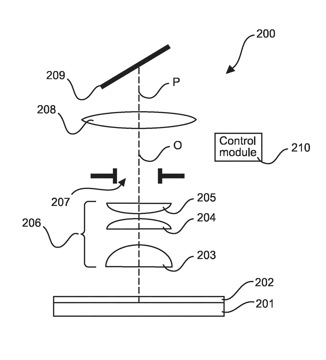
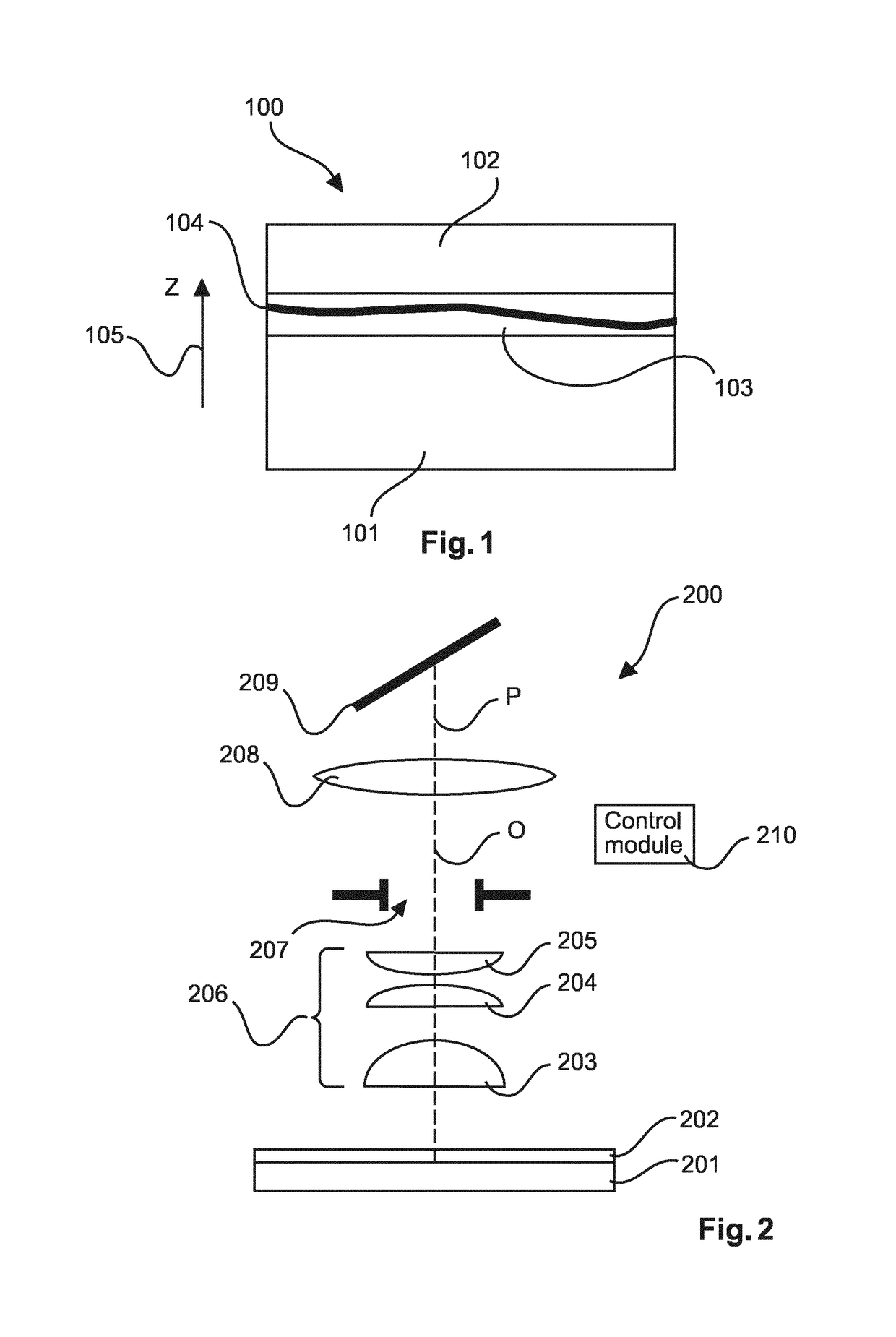
[0042]In the following, another exemplary, non-limiting embodiment of the present invention is provided by means of an imaging sensor which is described in thorough detail in the following table. Therein, the gap is described as “Gap Region” and is named “Pixel Pitch”, being the 13 pixel wide gap as described before. The pixels are rectangular as they are 5.56 micrometer long in Y direction and 6.42 micrometer in X direction, as can be seen from the following table.

[0043]

ParameterTypicalUnitPixel Size y5.56umPixel Size x6.42umPixel Pitch x (TDI)6.42umPixel Pitch x (Gap region)83.46um(13 pixel)Number of pixels in x direction (per TDI block)4Number of pixels in y direction4096Number of TDI blocks in x direction128Number of dark and test pixels x (per TDI4block)Number of dark and test pixels x (total)513Number of dark and test pixels y (per side)32Number of dark and test pixels y64Total number of effective pixels per line4096Total number pixels on Matrix4160 × 513DSNU 1%PRNU 2%Geometri...


PUM


Abstract

An imaging sensor comprising a 2D array of pixels in an XY coordinate system with gaps for electronic circuitry is presented. Furthermore, a scanning imaging system for imaging an oblique cross section of a sample with such a sensor is provided. Especially when the imaging sensor is in a tilted configuration this sensor is of specific advantages. The sensor allows for maximizing the photoactive part of the pixels in the photosensitive area of the sensor which leads to a maximized the fill factor. Furthermore this leads to a very light sensitive sensor and hence microlenses can be avoided. The gap or gaps of the imaging sensor facilitate also a faster read out because more circuitry can be positioned on the imaging sensor within the gap.

Description

CROSS-REFERENCE TO PRIOR APPLICATIONS[0001]This application is the U.S. National Phase application under 35 U.S.C. § 371 of International Application No. PCT / EP2014 / 077661, filed on Dec. 15, 2014, which claims the benefit of European Patent Application No. 13197416.4, filed on Dec. 16, 2013. These applications are hereby incorporated by reference herein.FIELD OF THE INVENTION[0002]The present invention relates to the field of imaging a sample, and applies advantageously in the field of digital pathology.[0003]In particular, the present invention relates to an imaging sensor comprising a 2D array of pixels, a scanning imaging system for imaging an oblique cross-section of a sample and the use of an imaging sensor in a digital scanning microscope.BACKGROUND OF THE INVENTION[0004]A digital scanning microscope usually makes a digital image of a sample such as a tissue sample placed in a microscope slide. This is typically done by scanning the sample over the whole microscope slide and s...

Claims


Application Information

Patent Timeline
Patent Type & Authority Patents(United States)
IPC IPC(8): H04N5/374H04N5/369G02B21/00G02B21/36H04N25/00
CPCH04N5/3743G02B21/002G02B21/365H04N5/369H04N25/768H04N25/70
Inventor HULSKEN, BAS
Owner KONINKLJIJKE PHILIPS NV
Learn More