
Pixel array, imaging sensor including the pixel array and digital camera including the imaging sensor

a technology of imaging sensor and array, applied in the field of image sensors, can solve the problems of reducing the light intensity of each sensor, directly related to the surface area of the photodiode, affecting the image quality of the image, and the noise of the chip, so as to improve the sensitivity of the cmos imaging sensor, improve the low light sensitivity, and reduce the noise of the cmos sensor imag

Active Publication Date: 2010-10-26
GLOBALFOUNDRIES U S INC
View PDF28 Cites 23 Cited by
  • Summary
  • Abstract
  • Description
  • Claims
  • Application Information

AI Technical Summary

Benefits of technology

[0009]It is another purpose of this invention to improve low light sensitivity for CMOS imaging sensor;
[0010]It is yet another purpose of the invention to reduce noise in CMOS sensor images at low light;
[0011]It is yet another purpose of the invention to reduce CMOS sensor image noise, while improving CMOS imaging sensor low light sensitivity.
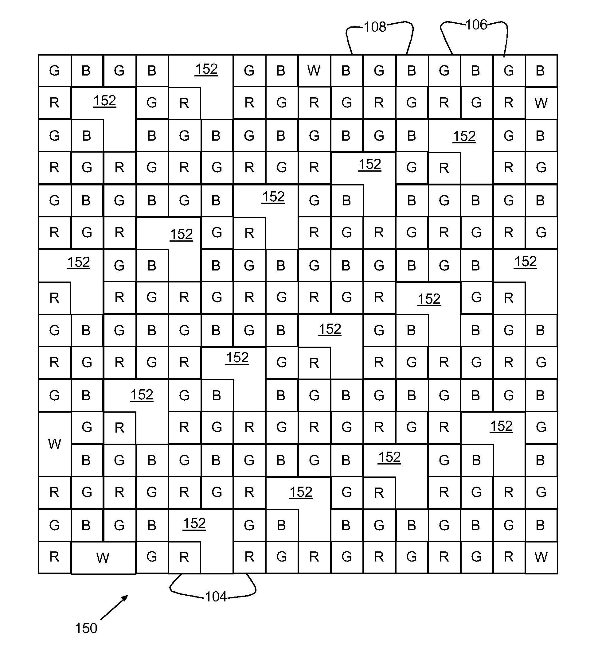
[0012]The present invention is related a pixel array in an image sensor, the image sensor and a digital camera including the image sensor. The image sensor includes a pixel array with colored pixels and unfiltered (color filter-free) pixels. Each unfiltered pixel occupies one or more array locations. The colored pixels may be arranged in uninterrupted rows and columns with unfiltered pixels disposed between the uninterrupted rows and columns. The image sensor may be implemented in CMOS with the unfiltered pixels reducing low-light noise and improving low-light sensitivity.

Problems solved by technology

Unfortunately, as pixel areas have shrunk to improve density, the amount of light to each sensor, which is directly related to photodiode surface area, has also diminished.
So for CMOS sensors in particular, as pixel density has increased, the diminished sensor light (sensor signal) may be lost in chip noise, especially in low light conditions.
For example, compact cameras with 6-8MP resolution, have been criticized for noisy results, even for pictures taken at sensitivity settings as low as 100 (ISO 100).
Thus, this noise is an impediment to increasing pixel density for CMOS imaging sensors, while maintaining a small chip footprint for compact applications.

Method used


Image

  • Pixel array, imaging sensor including the pixel array and digital camera including the imaging sensor
  • Pixel array, imaging sensor including the pixel array and digital camera including the imaging sensor
  • Pixel array, imaging sensor including the pixel array and digital camera including the imaging sensor

Examples


Embodiment Construction

[0018]Turning now to the drawings, and more particularly, FIG. 1 shows a first example of a color pixel array 100, wherein unfiltered photosensors or light efficient cells (LECs) 102 are included with red, green or blue filtered photosensor cells or pixels 104, 106 and 108, respectively, for improved sensitivity according to a preferred embodiment of the present invention. In this example, the pixels 102, 104, 106 and 108, are all of substantially equal size, each occupying a single array location. Also, the array 100 includes an equal number of each pixel type 102, 104, 106 and 108, such that 25% of the array is light efficient cells 102. Further in this example, the photodiodes 102, 104, 106 and 108 are arranged into red-green pixel rows 110 and blue-green pixel columns 112 bordering each LEC 102 and forming blue-LEC pixel rows 114 and red-LEC pixel columns 116.

[0019]Since the filters block light outside of the filtered spectrum from reaching the photosensors for the color filtere...


PUM


Abstract

A pixel array in an image sensor, the image sensor and a digital camera including the image sensor. The image sensor includes a pixel array with colored pixels and unfiltered (color filter-free) pixels. Each unfiltered pixel occupies one or more array locations. The colored pixels may be arranged in uninterrupted rows and columns with unfiltered pixels disposed between the uninterrupted rows and columns. The image sensor may in CMOS with the unfiltered pixels reducing low-light noise and improving low-light sensitivity.

Description

BACKGROUND OF THE INVENTION[0001]1. Field of the Invention[0002]The present invention generally relates to image sensors and more particularly to high resolution image sensors.[0003]2. Background Description[0004]Digital cameras have largely replaced film based analog cameras, at least for amateur photography. A typical digital camera image sensor is an array of picture cells (pixels), each sensing a small fragment of the light for an entire image. Generally, the higher the number of pixels, the better the resulting images (pictures) and the larger an image may be viewed before becoming pixilated. Thus, the number of pixels is a primary measure of the image resolution, and directly affects the sharpness and crispness of the resulting images. Early digital cameras included bucket brigade sensors with Charge Coupled Devices (CCDs) for pixel sensors. Integration, power, and frame rate considerations have driven the industry to convert from CCDs to image sensors that are based on more s...

Claims


Application Information

Patent Timeline
Patent Type & Authority Patents(United States)
IPC IPC(8): H04N3/14H04N5/335H04N9/04H04N9/083
CPCH04N9/045H04N25/133H04N25/135
Inventor ELLIS-MONAGHAN, JOHN J.JAFFE, MARK D.LOISEAU, ALAINRASSEL, RICHARD J.
Owner GLOBALFOUNDRIES U S INC
Learn More