
Laminated semiconductor substrate and process for producing the same

一种制造方法、衬底的技术,应用在半导体/固态器件制造、半导体器件、电固体器件等方向,能够解决活性层金属污染、长处理时间、工艺复杂等问题,达到提高生产率、降低成本、缩短处理时间的效果

Inactive Publication Date: 2007-01-10
SUMCO CORP
View PDF3 Cites 15 Cited by
  • Summary
  • Abstract
  • Description
  • Claims
  • Application Information

AI Technical Summary

Problems solved by technology

Thus, with this oxide film removal method, the process becomes complicated and a long processing time is required
In addition, the cost is also likely to be high
Moreover, due to the accompanying heat treatment, there is also the possibility of metal contamination of the active layer

Method used


Image

  • Laminated semiconductor substrate and process for producing the same
  • Laminated semiconductor substrate and process for producing the same
  • Laminated semiconductor substrate and process for producing the same

Examples


Embodiment 2

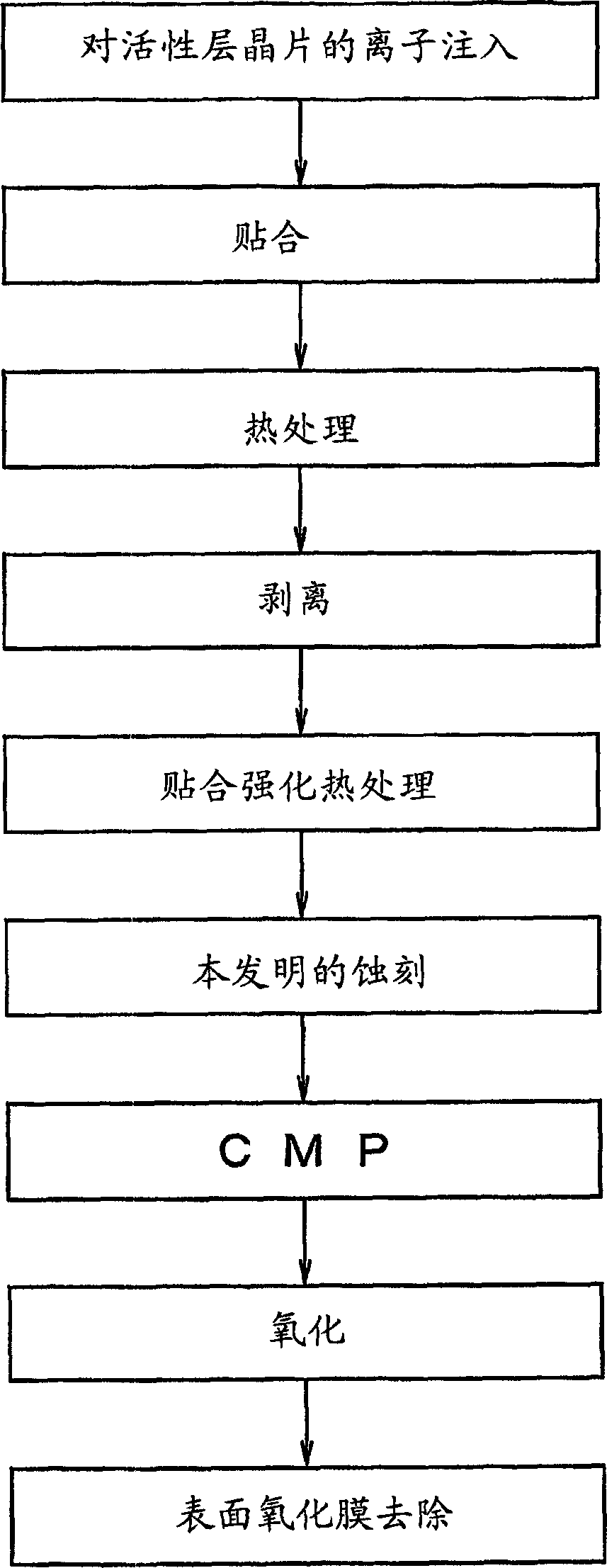
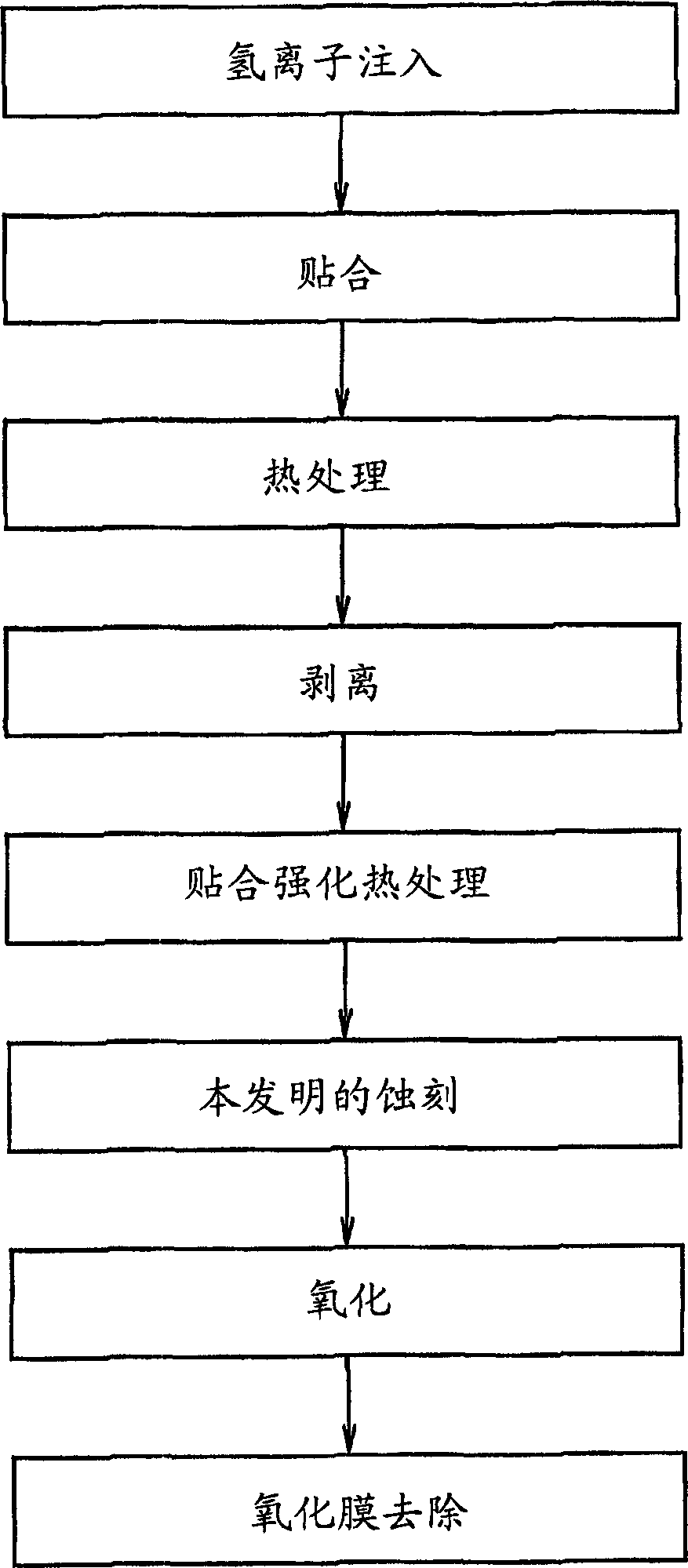
[0093] Embodiment 2 is an example as follows: In the second embodiment, the same procedure as that of the first embodiment is adopted, through hydrogen ion implantation to the wafer for the active layer, bonding of the wafer for the active layer and the wafer for the support substrate, and bonding of the wafer for the support substrate. The peeling heat treatment for forming bubbles of the bonded wafer, the peeling of the ion-implanted part of the wafer for the active layer, the bonding heat treatment for improving the bonding strength of the bonded wafer, etc., use the SC-1 cleaning solution to etch only the active layer surface. specified amount. Afterwards, CMP treatment, oxidation and oxide film removal are sequentially performed on the surface of the active layer.

[0094] At this time, the surface roughness of the active layer immediately after peeling was 6.17 nm (Rms).

[0095] The above-mentioned SC-1 etching was performed for 135 minutes using the same liquid compos...


PUM

PropertyMeasurementUnit
diameteraaaaaaaaaa
roughnessaaaaaaaaaa
roughnessaaaaaaaaaa

Abstract

The surface of an active layer of laminated substrate having undergone ionic implantation, laminating and detachment by heat treatment is etched by a thickness of 1 nm to 1 mum with the use of a solution having etching activity so that the final thickness of the active layer is 200 nm or less. Use is made of solution SC-1. Polishing, hydrogen annealing and sacrificial oxidation can be conducted before or after the etching. As a result, the thickness of thin-film active layer can be uniformalized over the entire surface thereof, and the surface roughness thereof can be reduced.

Description

technical field [0001] The present invention relates to a bonded semiconductor substrate and a method of manufacturing the same. Specifically, it relates to an active layer formed by peeling off a part of the active layer substrate. In particular, the thickness of the active layer film is as thin as 0.2 μm or less, and no active layer is formed. A bonded semiconductor substrate having a uniform thickness over its entire surface and a method of manufacturing the same. Background technique [0002] Bonded semiconductor substrates have been extensively studied especially in the field of semiconductors because they bond a support substrate and an active layer substrate having properties different from it, and make it have properties different from those of a single support substrate (Non-Patent Document 1 ). A typical example of a bonded substrate is an SOI (Silicon On Insulator) substrate. Among SOI substrates, a polished wafer (PW) of silicon is generally used as its support...

Claims


Application Information

Patent Timeline
Patent Type & Authority Applications(China)
IPC IPC(8): H01L27/12H01L21/02H01L21/306H01L21/762
CPCH01L21/30608H01L21/76254H01L21/20H01L27/12
Inventor 神山荣治加藤健夫朴在勤
Owner SUMCO CORP
Learn More