Checking method and method for preparation liquid crystal display device using the same

An inspection method and area technology, which is applied in semiconductor/solid-state device manufacturing, photo-plate-making process exposure device, optics, etc., can solve problems such as difficult to distinguish display unevenness, and achieve the effect of improving seam precision

Inactive Publication Date: 2006-12-06
MITSUBISHI ELECTRIC CORP
View PDF2 Cites 4 Cited by
  • Summary
  • Abstract
  • Description
  • Claims
  • Application Information

AI Technical Summary

Problems solved by technology

[0006] In Patent Document 1 and Patent Document 2, by arbitrarily mixing the part exposed when exposing one area and the part exposed when exposing the other area in the overlapping area, one area and the other area are not aligned in a straight line. Stitching, making it hard to tell the unevenness caused by seam offset

Method used


Image

  • Checking method and method for preparation liquid crystal display device using the same
  • Checking method and method for preparation liquid crystal display device using the same
  • Checking method and method for preparation liquid crystal display device using the same

Examples


Embodiment 1

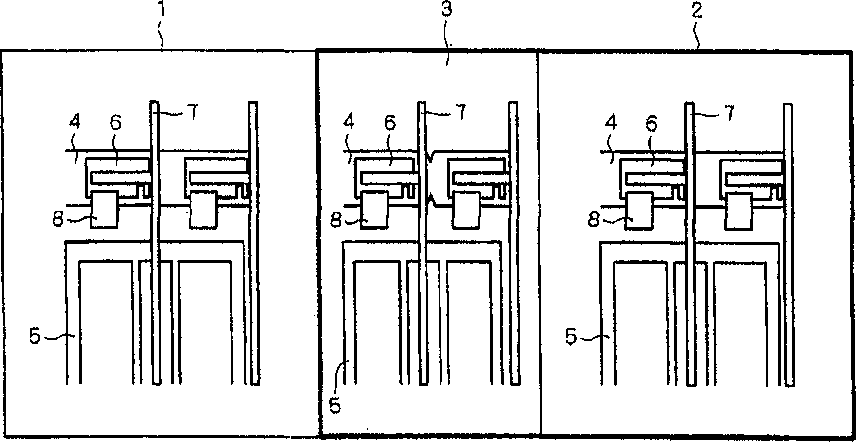
[0035] In the case where the predetermined pattern is formed by dividing the substrate into multiple regions and exposing them respectively, especially, in this embodiment, as figure 1 As shown in (a), two regions are provided, and each region is exposed using a mask to form one pattern on the substrate. figure 1 (a) shows a region 1 indicated by a thin line on the left and an area 2 indicated by a thick line on the right. When exposing area 1 and area 2 on the substrate, it is not simply exposing area 1 and area 2 side by side, but as figure 1 As shown in (b), exposure is provided with an overlapping region 3 in which region 1 and region 2 overlap. In addition, it does not matter whether to start exposure from area 1 or to start exposure from area 2. In addition, the overlapping region 3 is a mixture of a region that is exposed when the region 1 is exposed but not exposed when the region 2 is exposed, and a region that is exposed when the region 2 is exposed but not exposed...

Embodiment 2

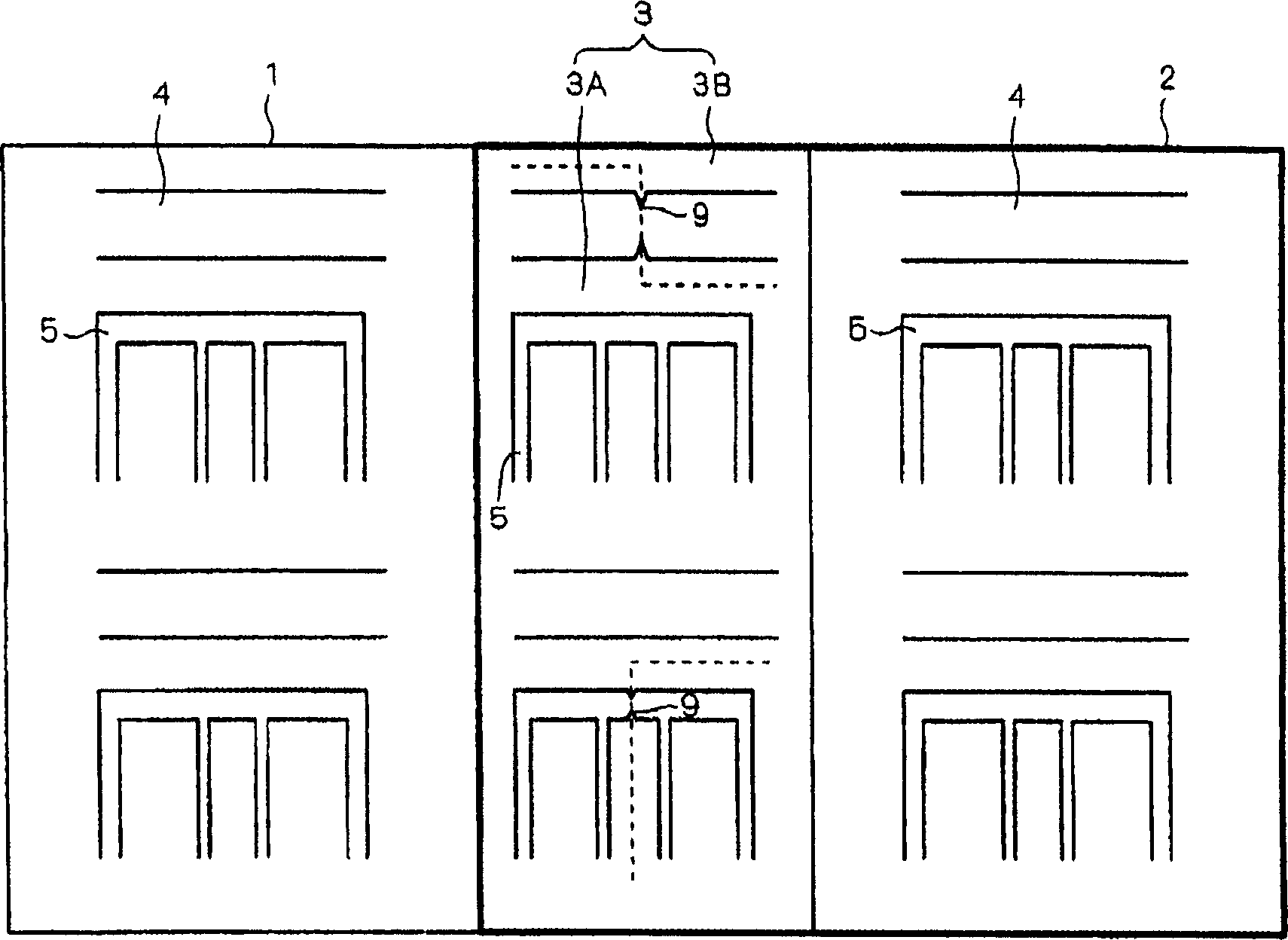
[0052] In this embodiment, another inspection method different from the inspection method shown in Embodiment 1 is shown. In addition, in this embodiment, the substrate is also divided into a plurality of regions and then exposed respectively to form predetermined patterns. Therefore, if figure 1 As shown in (a), a predetermined pattern is patterned on the substrate by dividing the region 1 and the region 2 . However, the region 1 and the region 2 are not patterned entirely in the region, but are patterned only in a part of the region (hereinafter also referred to as a pixel portion), and the rest are non-pattern forming portions where no pattern is formed. Also, the pixel portion constitutes a part of a predetermined pattern formed on the substrate.

[0053] Specifically, Figure 8 Masks for region 1 and region 2 are shown. Figure 8 In the shown mask, a mask pattern for exposing the pixel portion 12 is provided at the center. Then, Figure 8 In the shown mask, measurem...


PUM


Abstract

The invention provides a method for checking and increasing joint accuracy of pattern and process of producing liquid crystal display device employing said checking method. The method forms intended pattern by exposing substrate areas and then checks pattern joint accuracy with different exposure, and it comprises following steps: measuring the first pattern factor exposed at the first area in overlapped area of the first area and the second area, and measuring the first distance of the second pattern factor relevant to the first area exposure which is allocated paralleled to the first pattern factor; measuring the third pattern factor sewed with the first pattern factor relevant to the second area exposure and the second distance of the second pattern factor; computing differential value of the first and second distance and measuring quantification of joint accuracy.

Description

technical field [0001] The present invention relates to an inspection method and a method for manufacturing a liquid crystal display device using the method, and in particular to a method for inspecting seams when a predetermined pattern is formed by dividing a substrate into a plurality of regions and exposing them separately, and a liquid crystal display device using the inspection method manufacturing method. Background technique [0002] Generally, in a liquid crystal display device using a TFT (Thin Film Transistor), a TFT formed by photolithography is provided on one substrate. Photolithography uses an exposure device to form a predetermined pattern on a substrate, but it is difficult to uniformly expose with a mask when the substrate is large. Therefore, as the size of the substrate increases, it is necessary to divide the substrate into a plurality of regions, perform exposure using a plurality of masks, and form a predetermined pattern. [0003] However, when the ...

Claims


Application Information

Patent Timeline
Patent Type & Authority Applications(China)
IPC IPC(8): G03F7/20G02F1/1333
CPCG02F1/1303G02F1/1309G02F1/133516G02F1/133354H01L21/027
Inventor 山下敏广
Owner MITSUBISHI ELECTRIC CORP
Why Eureka
Try Eureka