
Patsnap Eureka
For R&D, Patsnap Eureka makes reading and utilizing patents & technical documents easy.
Patsnap Eureka AIR
Designed for self-driven R&D workflows. Generate viable solutions, solve complex R&D challenges, empower your innovation with AI.

Patsnap Eureka Materials
Designed for material experts only. Revolutionize your material R&D, from search, analyze, to developing new materials.

TechResearch
Generate reliable direction feasibility study reports for your R&D in just a few steps.

TechSeek
Discover and master advanced knowledge NOW. Basics, ideas, possibilities, all at once.

TechMind
As an expert in R&D Theories, TechMind can generates customized viable solutions instantly.

TechRisk
Analyze your overall solution with one click, know your potential R&D risks in advance.

TechMonitor
Get weekly tech updates, stay abreast of the latest tech innovations and key insights.
Electro-optical device, manufacturing method thereof, and electronic apparatus
A technology of electro-optical devices and side electrodes, which is applied to identification devices, optics, circuits, etc., and can solve problems such as reduced light-shielding performance, reduced display quality, and complicated manufacturing methods
- Summary
- Abstract
- Description
- Claims
- Application Information
AI Technical Summary
Problems solved by technology
Method used
Image

Examples
no. 1 Embodiment approach
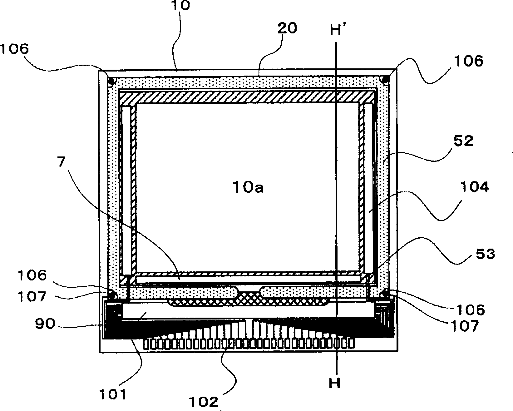
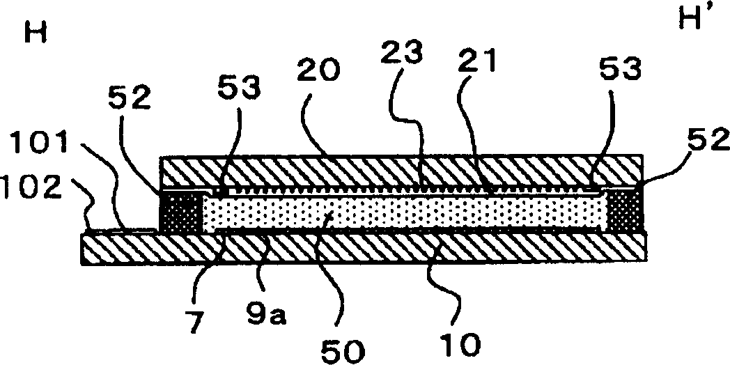
[0051] For the liquid crystal device of the first embodiment of the present invention, refer to Figure 1 ~ Figure 1 0 for explanation.
[0052] First, refer to figure 1 and figure 2 , the overall configuration of the liquid crystal device of this embodiment will be described. it's here, figure 1 is a plan view showing the overall structure of the liquid crystal device of this embodiment, figure 2 yes figure 1 Sectional view at line H-H'.
[0053] exist figure 1 and figure 2 In the liquid crystal device of this embodiment, the TFT array substrate 10 and the counter substrate 20 are arranged facing each other. A liquid crystal layer 50 is sealed between the TFT array substrate 10 and the opposing substrate 20, and the TFT array substrate 10 and the opposing substrate 20 are arranged around the image display region 10a as an example of the "pixel array region" of the present invention. The sealing material 52 of the sealing area is bonded to each other.
[0054] exi...
PUM
 Abstract
Description
Claims
Application Information
 - R&D Engineer
- R&D Manager
- IP Professional
- Industry Leading Data Capabilities
- Powerful AI technology
- Patent DNA Extraction
Browse by: Latest US Patents, China's latest patents, Technical Efficacy Thesaurus, Application Domain, Technology Topic, Popular Technical Reports.
© 2024 PatSnap. All rights reserved.Legal|Privacy policy|Modern Slavery Act Transparency Statement|Sitemap|About US| Contact US: help@patsnap.com