
Access buffer storaging method

A cache and buffer technology, which is applied in the direction of synchronous signal speed/phase control, etc., can solve the problems of reducing the complexity of the logic circuit design of the first-in-first-out buffer, the uncertainty of the delay error of the first-in-first-out buffer, etc., and achieve the reduction of delay changes range, effect of guaranteed constancy

Inactive Publication Date: 2006-08-02
HUAWEI TECH CO LTD
View PDF0 Cites 8 Cited by
  • Summary
  • Abstract
  • Description
  • Claims
  • Application Information

AI Technical Summary

Problems solved by technology

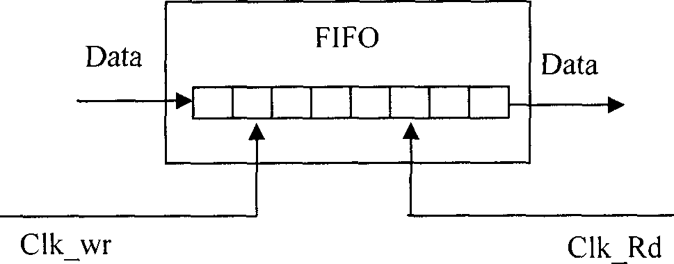
[0011] The purpose of the present invention is to provide a method for accessing the buffer to solve the problem of uncertain delay error of the first-in-first-out buffer due to clock jitter when data transmission is performed between two boards with no relative frequency difference between the receiving and sending clocks. Using this method can ensure that the delay error of the FIFO does not exceed the jitter range of the clock, and at the same time reduce the design complexity of the logic circuit of the FIFO

Method used


Image

  • Access buffer storaging method
  • Access buffer storaging method
  • Access buffer storaging method

Examples


Embodiment Construction

[0032] The present invention will be described in further detail below in conjunction with the accompanying drawings.

[0033] The technical solution of the present invention is based on the premise that both the read clock and the write clock are locked on the same clock source, and the frequencies of the sending and receiving clocks are the same, but there is a certain range of phase jitter.

[0034] Such as Figure 4As shown, the present invention at first arranges n cache units on the FIFO buffer, n=[x]+2, wherein [x] represents that the relative jitter range of the read-write clock is rounded up, and the relative jitter range of the read-write clock is equal to or greater than The multiple of the clock cycle is the unit; set the write clock flag signal and the read clock flag signal respectively, the cycle of the write clock flag signal is n times the write clock cycle, and the cycle of the read clock flag signal is n times the read clock cycle; All cache units are writt...


PUM


Abstract

This invention discloses a kind of method for accessing buffer store. Through arranging n buffer cells, write clock identification signal which cycle is n times write clock cycle and read clock identification signal which cycle is n times read clock cycle on the first-in first-out buffer, all the buffer cells are undertaken write operation successively during write clock signal cycle. When writing the first buffer cell, the write clock signal is high level, the others are low level; the write clock identification signals are sampled during the rising edge of each write clock cycle, which is in the write clock identification signal cycle. The rising edge position of the write clock identification signal is decided according to the sampled consequence; the buffer cells are began to undertaken read operation from at least the second read clock cycle after the write clock cycle corresponded to the rising edge of write clock identification signal. This method can ensure that the delay error does not exceed clock jittering range. The designing complexity of logical circuit is decreased.

Description

technical field [0001] The present invention relates to cache, in particular to a method for accessing cache. Background technique [0002] In many fields such as 3G mobile communication base stations, the delay accuracy requirements of signals in hardware are often very strict. For example, in the 3GPP protocol specification of the WCDMA (Wide-band Code Division Multiple Access, wideband code division multiple access) system, it is required that the relative delay error between the signals on the two antennas of the transmit diversity should not exceed 1 / 4 chip (approximately 65ns), Another example is in the CPRI (Common Public Radio Interface, common public radio interface) protocol, requiring REC (Radio Equipment Control, radio frequency equipment controller) equipment to RE (Radio Equipment, radio frequency equipment) equipment hardware interface delay accuracy better than 1 / 32chip (approximately 8ns). This not only has high requirements on the delay consistency of an...

Claims


Application Information

Patent Timeline
Patent Type & Authority Applications(China)
IPC IPC(8): H04L7/08
Inventor 李刚
Owner HUAWEI TECH CO LTD
Learn More