
Methdo for fabricating bipolar type longitudinal plane mode transistors

A vertical plane and manufacturing method technology, applied in semiconductor/solid-state device manufacturing, electrical components, circuits, etc., can solve problems such as high collector saturation voltage drop, large collector circuit series resistance, and affecting circuit integration density

Inactive Publication Date: 2006-07-05
SHANGHAI BEILING
View PDF0 Cites 1 Cited by
  • Summary
  • Abstract
  • Description
  • Claims
  • Application Information

AI Technical Summary

Problems solved by technology

In this way, the area of ​​the transistor increases, which affects the integration density of the circuit.
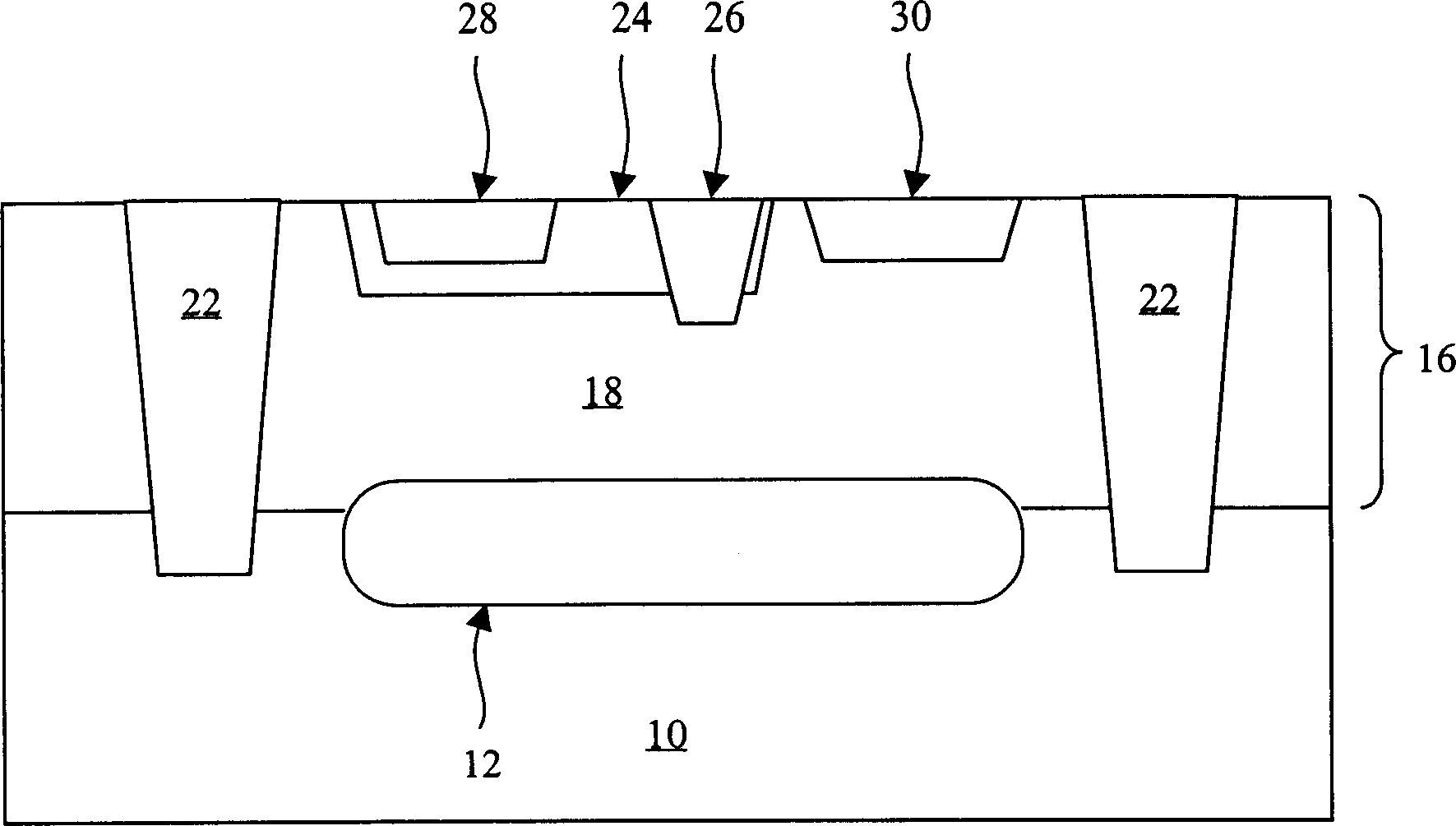
[0010] 2) Connecting the extrinsic collector region 12 and the collector region 30 is a low-concentration doped N-type epitaxial layer 16. In this way, the series resistance of the collector circuit is relatively large, so the collector saturation voltage drop is relatively high
The dielectric film layer is usually obtained by chemical vapor deposition, and the production cost is relatively high

Method used


Image

  • Methdo for fabricating bipolar type longitudinal plane mode transistors
  • Methdo for fabricating bipolar type longitudinal plane mode transistors
  • Methdo for fabricating bipolar type longitudinal plane mode transistors

Examples


Embodiment Construction

[0026] Figure 5 It is a sectional view of an NPN-type bipolar vertical planar transistor of the present invention. See Figure 5 , forming an N-type extrinsic collector region 52 on the top of the P-type semiconductor substrate 50; doping a P-type impurity element in the semiconductor substrate surrounding the extrinsic collector region 52 as a lower isolation layer 54 of the transistor; A part of the N-type epitaxial layer 56 is used as the intrinsic collector region 58 of the transistor; an N-type impurity element is doped on the top of the epitaxial layer 56 as a plug 60 connecting the extrinsic collector region 52; on the top of the epitaxial layer 56 P-type impurity elements are doped as the upper isolation layer 62 of the isolation transistor, and the upper isolation layer 62 and the lower isolation layer 54 are overlapped, and after a certain high temperature treatment, the upper and lower isolation layers are connected to play an isolation role; The top of layer 56 ...


PUM


Abstract

The method includes steps: selecting a semiconductor substrate; forming non-intrinsic collector region in the semiconductor substrate; forming preparative layer of lower isolation layer of isolation transistor in the semiconductor substrate; forming intrinsic collector region on the non-intrinsic collector region; forming the lower isolation layer on the intrinsic collector region; on the intrinsic collector region, forming male contact to connect to non-intrinsic collector region; forming a upper isolation layer; forming following regions: intrinsic base region on the intrinsic collector region, and non-intrinsic base region on the intrinsic base region; forming emitter region on intrinsic base region and forming collector region on the male contact. Features are: using two isolation layers make area of transistor smaller; small block resistance on intrinsic base region; low saturation voltage of collector; obtaining dielectric film for protecting transistor through saving method.

Description

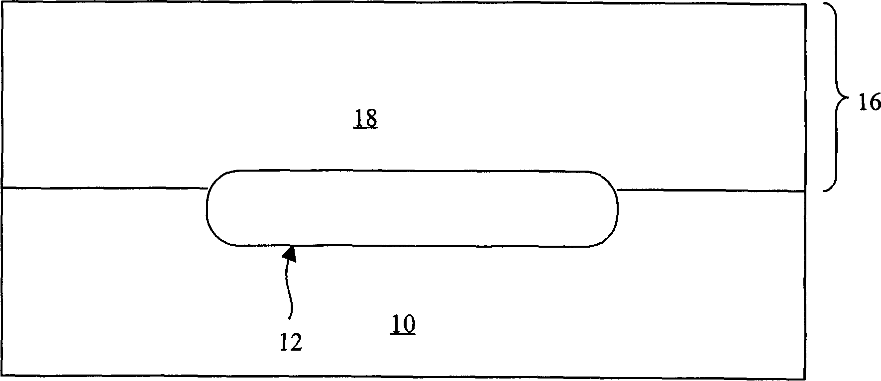
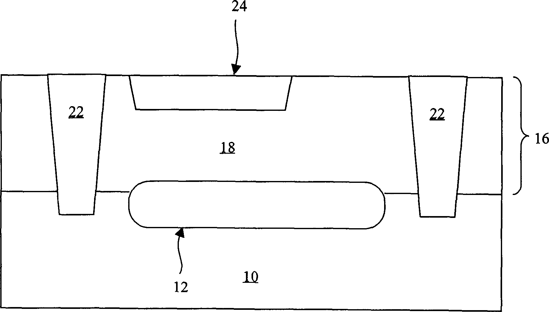
technical field [0001] The invention relates to a method for manufacturing a bipolar longitudinal planar semiconductor transistor, in particular to a method for manufacturing a bipolar longitudinal planar transistor suitable for large-scale integrated circuits requiring low noise and strong current drive capability. Background technique [0002] Transistor is an active device that plays an important role in integrated circuits. It has various uses, such as constant voltage source, constant current source, small signal amplifier, high current driver, etc. Therefore, the performance of a transistor directly affects the function of the integrated circuit. Integrated circuits with different functions have different requirements on transistor performance. [0003] For large-scale integrated circuits with general requirements, the manufacturing method of its transistors can be found in Figure 1~4 , that is Figure 1~4 It is a sectional view of the manufacturing process of a comm...

Claims


Application Information

Patent Timeline
Patent Type & Authority Applications(China)
IPC IPC(8): H01L21/331
Inventor 张复才
Owner SHANGHAI BEILING
Learn More