Method of thermal adherend release and apparatus for thermal adherend release

A peeling device and adherend technology, applied in the direction of adhesives, electric solid devices, semiconductor devices, etc., can solve the problems of semiconductor wafer cracking, falling off, component displacement, etc., to prevent damage and displacement, accurate peeling, prevent productivity or production. rate reduction effect

Inactive Publication Date: 2006-06-14
NITTO DENKO CORP
View PDF7 Cites 16 Cited by
  • Summary
  • Abstract
  • Description
  • Claims
  • Application Information

AI Technical Summary

Problems solved by technology

However, it is difficult to reduce the bonding strength between the cut-out semiconductor wafer and the base material to such an extent that the semiconductor wafer can be easily picked up only by shrinking the base material
At the same time, in shrinkage, it is difficult to shrink the base material evenly in the machine direction and transverse direction
Therefore, there is a problem that the semiconductor wafer is displaced and comes into contact with an adjacent semiconductor wafer, causing the semiconductor wafer to crack
Furthermore, in the dicing step of semiconductor wafers or laminated capacitors, after the dicing operation, when the heat-peelable pressure-sensitive adhesive sheet holding these parts is heated to peel the parts, there are problems involved: Vibration generated during transfer and separation of parts, integral separation of parts including parts intended to be held and occurrence of part displacement or fall-off

Method used


Image

  • Method of thermal adherend release and apparatus for thermal adherend release
  • Method of thermal adherend release and apparatus for thermal adherend release

Examples


Embodiment 1

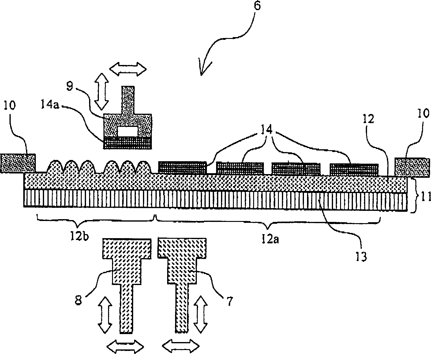
[0149] In the case composed of a polyester base material (thickness 100 μm) and a heat-expandable pressure-sensitive adhesive layer (whose peel strength decreases at 90°C (peeling initiation temperature is 90°C)) formed on one surface of the polyester base material In the heat-peelable pressure-sensitive adhesive tape (fixed by a fixing ring), a silicon wafer (thickness 150 µm) having a diameter of 6 inches was adhered to the surface of the heat-expandable pressure-sensitive adhesive layer without introducing air bubbles. Then, the aforementioned silicon wafer was cut into 3 mm size cubes.

[0150] In addition, a preheating zone in which a stainless steel (SUS 304) plate having a size of 3 mm square and a thickness of 2 mm and a thermally conductive rubber sheet (3 mm square and 1 mm thickness) and a stripping and heating zone were respectively prepared as the preheating zone and Peel and heat zone. Then, heating is performed by an electric heater so that the temperature of t...

Embodiment 2

[0154] The silicon wafer slices were peeled off in the same manner as in Example 1, except that a heat-peelable pressure-sensitive adhesive tape having a heat-expandable pressure-sensitive adhesive layer having a peeling start temperature of 120° C. was used as the heat-peelable pressure-sensitive adhesive tape. Sensitive adhesive tape, and use such conditions: the temperature of the rubber sheet portion (leading end portion) in the preheating zone is 105°C, and the temperature of the rubber sheet portion (leading end portion) in the peeling and heating zone is 170°C. In this case, when the slice of the silicon wafer was adsorbed and peeled by the suction nozzle, the time required to peel one slice of the silicon wafer (average time required for peeling) was 1.5 seconds, as shown in Table 1.


PUM

PropertyMeasurementUnit
melting pointaaaaaaaaaa
tensile modulusaaaaaaaaaa
widthaaaaaaaaaa

Abstract

A heat-adherent peeling method, wherein a part of an adherend adhered to a heat-peelable pressure-sensitive adhesive sheet having a heat-expandable layer containing a foaming agent is partially heated by partially heating the heat-peelable pressure-sensitive adhesive The adhesive sheet is selectively peeled from the pressure-sensitive adhesive sheet, wherein the method comprises preheating the adherend to be peeled off at a temperature at which the heat-expandable layer of the heat-peelable pressure-sensitive adhesive sheet does not expand. The adherend is then heated at the temperature at which the heat-expandable layer expands, thereby selectively peeling the adherend.

Description

technical field [0001] The present invention relates to a method of selectively peeling off a portion of an adherend by heating from a heat-peelable pressure-sensitive adhesive sheet having a heat-expandable layer, and a device for thermally peeling an adherend by the subject method. Background technique [0002] As a method of peeling a portion adhered to the pressure-sensitive tape from the pressure-sensitive tape after processing, for example, there is a method of picking up a semiconductor wafer prepared by shrinking a base material and dicing it (see Patent Document 1). However, it is difficult to reduce the bonding strength between the cut-out semiconductor wafer and the base material to such an extent that the semiconductor wafer can be easily picked up only by shrinking the base material. Meanwhile, in shrinking, it is difficult to shrink the base material uniformly in the machine direction and the transverse direction. Therefore, there is a problem that the semicon...

Claims


Application Information

Patent Timeline
Patent Type & Authority Applications(China)
IPC IPC(8): H01L21/00C09J7/38H01L21/67
CPCB29C63/0013C09J2203/326H01L21/6836H01L2221/68327H01L2924/19041Y10S438/976C09J7/38Y10T156/1147Y10T156/1153Y10T156/1911C09J2301/412C09J2301/502H01L21/82H01L21/78
Inventor 土井知子下川大辅有满幸生
Owner NITTO DENKO CORP
Why Eureka
Try Eureka