Logic circuit

A logic circuit and power supply technology, applied in the field of logic circuits, can solve the problems of longer transmission delay time and inability to cope with high speed, and achieve the effect of suppressing time lag

Inactive Publication Date: 2006-06-07
NEC ELECTRONICS CORP
View PDF1 Cites 1 Cited by
  • Summary
  • Abstract
  • Description
  • Claims
  • Application Information

AI Technical Summary

Problems solved by technology

This circuit is an exclusive OR circuit, which is composed of NOR gates, AND gates and other multi-level gate circuits. It is used to solve the problem that the transmission delay time becomes longer and cannot cope with high speed. The transmission gate composed of nMOS transistor NM11 and pMOS transistor PM11, which are respectively input from the gate to compare the data signal φ1 and the inversion signal of the comparison data signal φ1 through the inverter INV to accept on / off control, also has: source and The power supply VDD is connected, the gate is connected to the pMOS transistor PM12 of the input terminal RD; the source is connected to the drain of the pMOS transistor PM12, the gate is connected to the output of the inverter INV, and the drain is connected to the pMOS transistor PM13 of the output terminal CD; an nMOS transistor NM12 whose drain is connected to the output terminal CD, whose gate is connected to the input terminal of the comparison data signal φ1; and whose source is connected to the ground, whose drain is connected to the source of the nMOS transistor NM12, and whose gate is connected to the input terminal RD nMOS transistor NM13

Method used


Image

  • Logic circuit
  • Logic circuit
  • Logic circuit

Examples


Embodiment

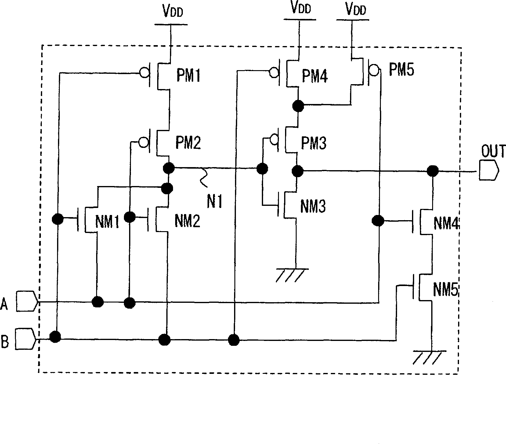
[0039] figure 1 It is a figure which shows the structure of the logic circuit of one Example of this invention. refer to figure 1 , an embodiment of the present invention has input terminals A and B respectively using logic signals as inputs, has sources connected to corresponding input terminals A and B respectively, and an nMOS transistor NM1 whose gate is cross-connected to input terminals B and A , NM2, and the drains of the nMOS transistors NM1 and NM2 are connected in common. Furthermore, there are pMOS transistors PM1, PM1, and NM1 connected in series between the power supply VDD and a node (referred to as a "common node") N1 at which the drains of nMOS transistors NM1 and NM2 are connected in common, and their gates are connected to input terminals B and A, respectively. PM2 also has an inverter composed of an nMOS transistor NM3 whose source is connected to ground and a pMOS transistor PM3 whose drain is connected to the drain of the nMOS transistor NM3 and whose ...


PUM


Abstract

A logic circuit that realizes shortened transmission delay time and can cope with high speed. It has the first and second input terminals (A, B) with logic signals as input, the sources are respectively connected to the corresponding first and second input terminals (A, B), and the gate is connected to the second and first inputs. The first and second MOS transistors (NM1, NM2) that are cross-connected to the terminals (B, A), and the drains of the first and second MOS transistors (NM1, NM2) are connected in common, and have the first power supply VDD and the first and second MOS transistors. The drains of the transistors (NM1, NM2) are connected to the common node (N1), the gate receives the reset signal ( / RESET), and the MOS transistor (PM1) that is turned on at reset also has an input terminal connected to the common node N1 inverter (INV).

Description

technical field [0001] The invention relates to a logic circuit, in particular to a logic circuit suitable for a data comparison circuit and a coincidence detection circuit. Background technique [0002] Figure 6 It is a diagram showing an example of the configuration of a conventional comparison and judgment circuit (exclusive OR circuit) (see Patent Document 1 described later). This circuit is an exclusive OR circuit, which is composed of NOR gates, AND gates and other multi-level gate circuits. It is used to solve the problem that the transmission delay time becomes longer and cannot cope with high speed. The transmission gate composed of nMOS transistor NM11 and pMOS transistor PM11, which are respectively input from the gate to compare the data signal φ1 and the inversion signal of the comparison data signal φ1 through the inverter INV to accept on / off control, also has: source and The power supply VDD is connected, the gate is connected to the pMOS transistor PM12 of...

Claims


Application Information

Patent Timeline
Patent Type & Authority Applications(China)
IPC IPC(8): H03K19/00G11C11/401
CPCH03K19/00323H03K19/215
Inventor 高桥弘行高野将
Owner NEC ELECTRONICS CORP
Why Eureka
Try Eureka