
Rectifier diode, chip special for producing rectifier diode and producing method

A technology of rectifying diodes and chips, which is applied in semiconductor/solid-state device manufacturing, electrical components, circuits, etc., can solve the problems of low withstand voltage of chips, and achieve the effects of stable performance, reduced leakage current, and faster speed

Active Publication Date: 2006-06-07
ANHUI PROVINCE QIMEN COUNTY HUANGSHAN ELECTRIC APPLIANCE
View PDF0 Cites 7 Cited by
  • Summary
  • Abstract
  • Description
  • Claims
  • Application Information

AI Technical Summary

Problems solved by technology

[0007] B. From the perspective of the single-sided groove structure, the groove passivation mesa of the chip is P + The mesa formed on the area is a negative bevel greater than 30 degrees, so the withstand voltage of the chip is low, generally only below 1400V

Method used


Image

  • Rectifier diode, chip special for producing rectifier diode and producing method
  • Rectifier diode, chip special for producing rectifier diode and producing method
  • Rectifier diode, chip special for producing rectifier diode and producing method

Examples


Embodiment

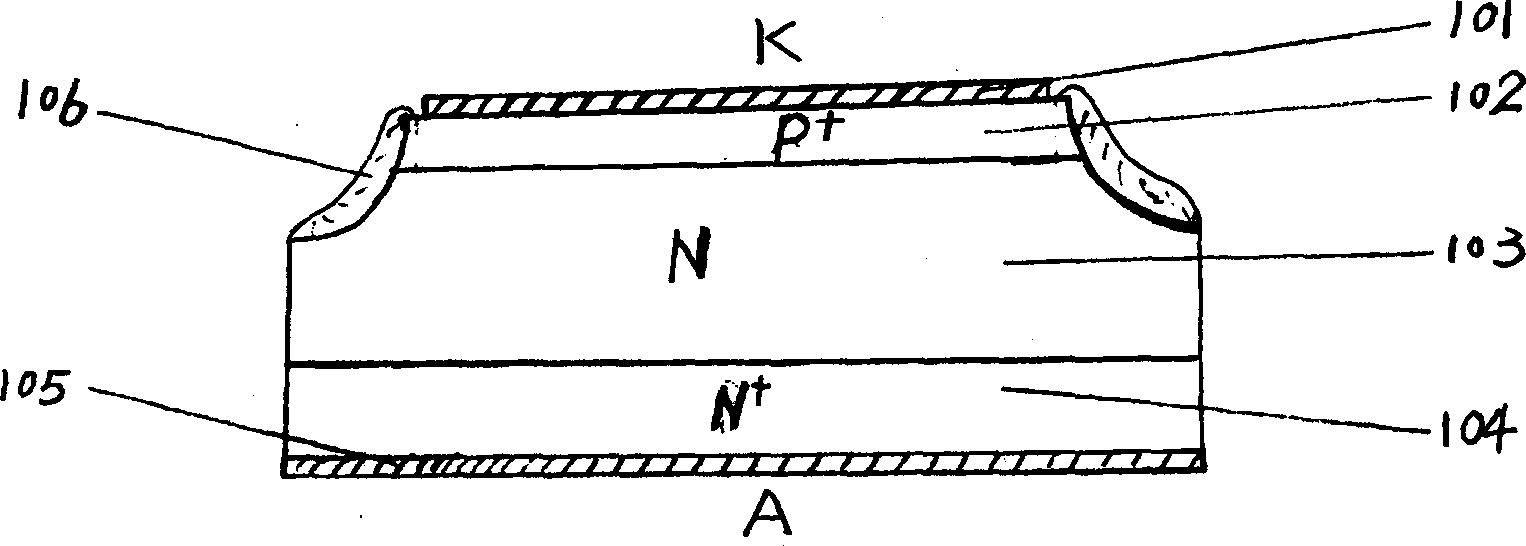
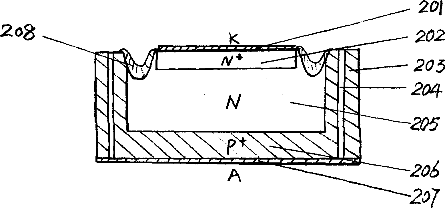
[0036] The rectifier diode is composed of three parts: the shell, the chip, and the lead wire. The core part is the chip, and the shell plays a protective role outside the chip. There are two lead wires on the anode and cathode of the chip. The chip includes a long base region N205, a phosphorous diffusion region N + 202. Concentrated boron diffusion area P + 206. Groove passivation table 208, separation wall 203, laser hole 204, cathode K201, anode A207, the middle of the chip is the long base area N205, and the upper part is the phosphorus diffusion area N + 202, the lower part is the concentrated boron diffusion area P + 206, the periphery of the chip is provided with a partition wall 203, a laser hole 204 vertically penetrated is provided on the plane of the partition wall 203, and the cathode K201 is in the phosphorus diffusion area N + 202, the anode A207 is on the concentrated boron diffusion region P+206, and the groove-type passivation mesa 208 is between the isolat...


PUM

PropertyMeasurementUnit
Diameteraaaaaaaaaa
Spacingaaaaaaaaaa

Abstract

This invention discloses a commutation diode, chips especially for manufacturing the diodes and the manufacturing method, in which, said commutation diode is composed of a shell, a chip and a lead out wire, in which, the chip includes a long base region N, a phosphor diffusion region N area, a heavy boron diffusion region P area and a groove passive mesa, the long base region is in the middle of the chip, cathode K is on the phosphor diffusion region, anode A is on the heavy boron diffusion region, the upper part is the P diffusion region, the lower part is the B diffusion region, isolation walls are surrounding the chip with vertical through laser holes in the diameter smaller than 200mum and the inter-distance of 40-400mum and the mesa is between the isolation wall and the cathode K.

Description

Technical field: [0001] The invention relates to the technical field of rectifying diodes, and more specifically relates to rectifying diodes, a chip specially used for manufacturing rectifying diodes and a manufacturing method thereof. Background technique: [0002] The power semiconductor device rectifier diode is mainly composed of a shell, a chip, and lead wires. The core part is the chip, and the shell protects the outside of the chip. There are two lead wires on the anode and cathode of the chip. The manufacturing method of the rectifier diode chip is generally divided into the grinding angle method and the single-sided groove method: [0003] 1. Angle grinding method: Since the traditional angle grinding method determines that the structure of the rectifier diode chip is circular, most of the production process can only be operated one by one, the proportion of manual operation is high, the production efficiency is low, and the labor intensity is high. Low utilizatio...

Claims


Application Information

Patent Timeline
IPC IPC(8): H01L29/861H01L21/329
Inventor 王日新
Owner ANHUI PROVINCE QIMEN COUNTY HUANGSHAN ELECTRIC APPLIANCE
Learn More