Solid-state image pickup device and drive method thereof
A driving method, solid-state imaging technology, applied in image communication, signal generator with a single pickup device, picture signal generator, etc., can solve problems such as increased folding noise
- Summary
- Abstract
- Description
- Claims
- Application Information
AI Technical Summary
Problems solved by technology
Method used
Image

Examples
no. 1 example
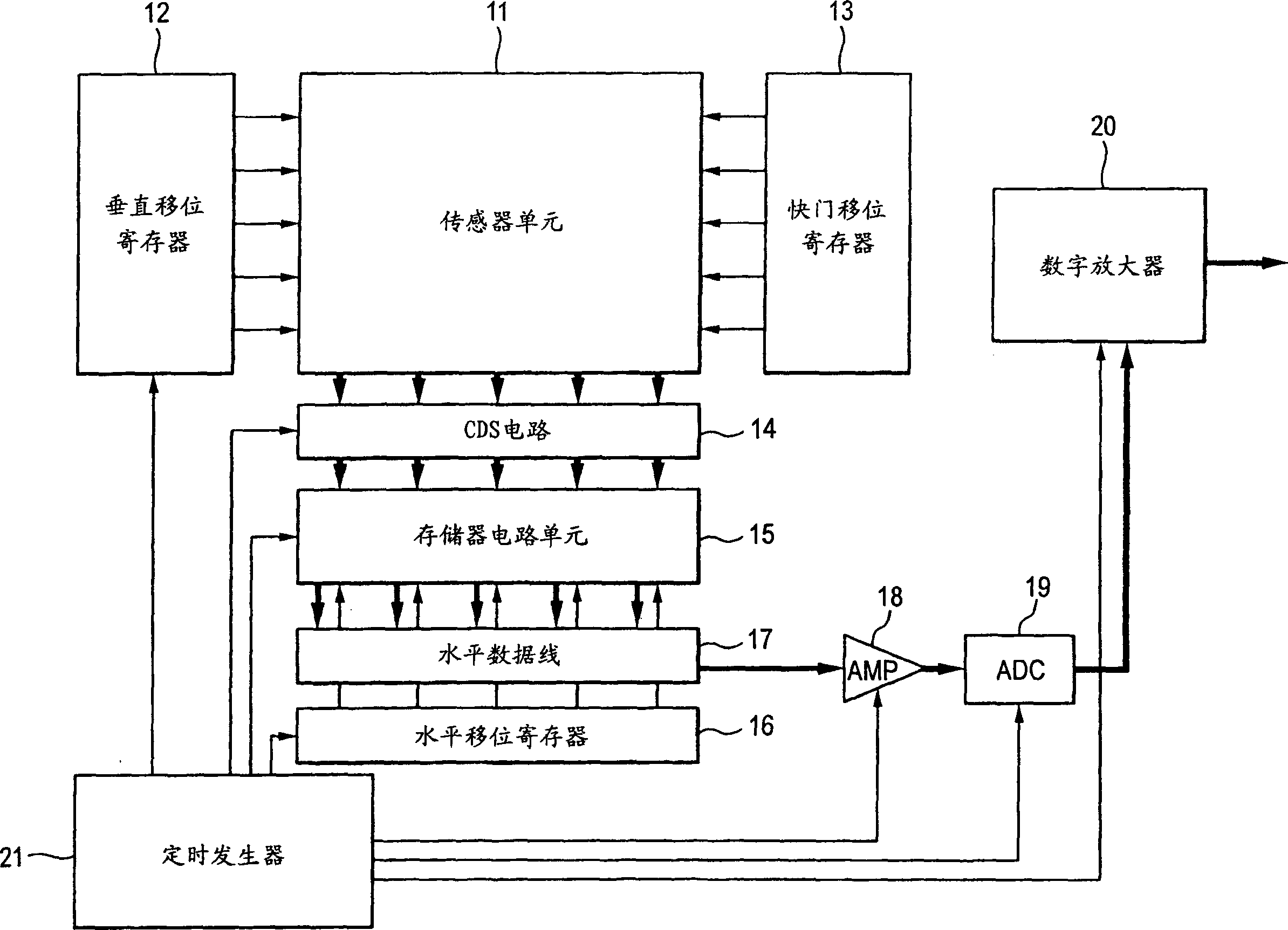
[0054] figure 1 is a block diagram showing an example of the structure of the solid-state imaging device according to the first embodiment of the present invention. In an example described in this embodiment, an X-Y addressable solid-state imaging device of a type for simultaneously reading out pixel information of one line, such as a CMOS image sensor, is used as the solid-state imaging device.
[0055] Such as figure 1 As shown, the solid-state imaging device according to this embodiment includes a sensor unit 11, a vertical shift register 12, a shutter shift register 13, a CDS (correlated double sampling) circuit 14, a memory circuit unit 15, a horizontal shift register 16, a horizontal A data line 17 , an amplifier unit (AMP) 18 , an AD converter (ADC) 19 , a digital amplifier 20 , and a timing generator 21 .
[0056] The sensor unit 11 has a structure in which pixels are arranged in a matrix and wiring row selection lines, shutter lines, vertical data lines, and the l...
no. 2 example
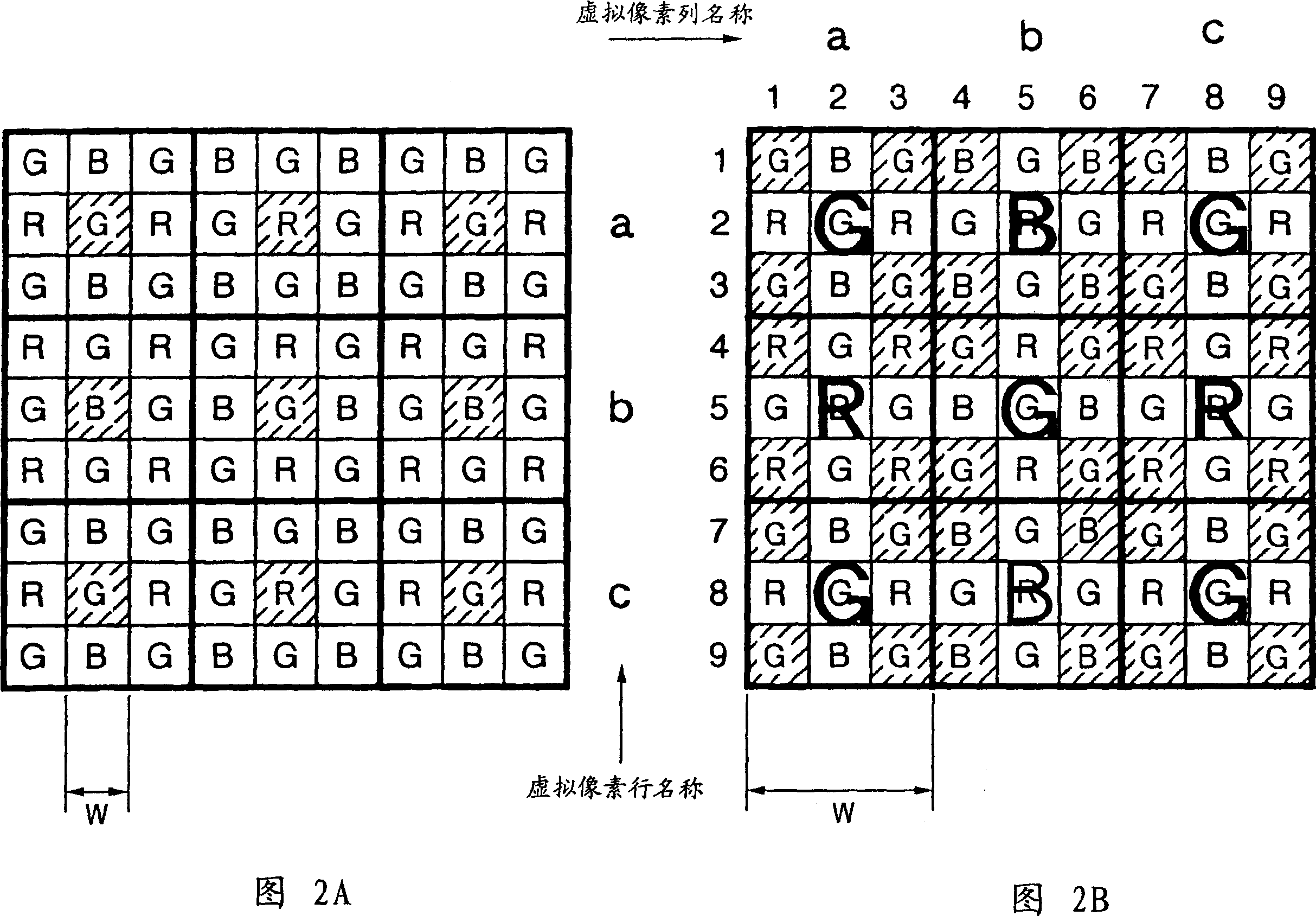
[0089] The structure of the solid-state imaging device according to the second embodiment of the present invention is basically the same as figure 1 The shown solid-state imaging device according to the first embodiment has basically the same structure. However, in the solid-state imaging device according to this embodiment, when k is a positive integer equal to or greater than 0, in the process of compressing the pixel information amount at a ratio of 1 / (k+2)×(k+2), (k+2)×(k+2) pixels are skip-added in a state where analog pixel blocks (unit pixel blocks) to be skip-added are arranged overlapping each other, whereby pixel information is skipped in a state where aliasing noise is reduced. The solid-state imaging device in this embodiment will be specifically exemplified with reference.
[0090] (first specific example)
[0091] In the case of the first specific example, k=0, in other words, four (2×2) pixels are skip-added and the pixel information amount is compressed at a...
no. 3 example
[0129] Figure 18 is a block diagram showing an example of the structure of the solid-state imaging device according to the third embodiment of the present invention. In this figure, the equivalent of figure 1 Those parts of the parts in . In the solid-state imaging device according to this embodiment, again, an X-Y addressable solid-state imaging device of a type for simultaneously reading out pixel information of one line, such as a CMOS image sensor, is used as the solid-state imaging device.
[0130] In the structure employed in the solid-state imaging device according to this embodiment, two memory circuits 15A and 15B capable of storing pixel information of one row in the sensor unit 11 are used as the memory circuit unit 15 . In this respect, the solid-state imaging device according to this embodiment is different from the solid-state imaging device according to the first embodiment in terms of the structure. The solid-state imaging device according to this embodime...
PUM
 Abstract
Description
Claims
Application Information
 - R&D
- Intellectual Property
- Life Sciences
- Materials
- Tech Scout
- Unparalleled Data Quality
- Higher Quality Content
- 60% Fewer Hallucinations
Browse by: Latest US Patents, China's latest patents, Technical Efficacy Thesaurus, Application Domain, Technology Topic, Popular Technical Reports.
© 2025 PatSnap. All rights reserved.Legal|Privacy policy|Modern Slavery Act Transparency Statement|Sitemap|About US| Contact US: help@patsnap.com