Semiconductor packaging with partially patterned lead frames and its making methods

A lead frame and frame technology, which is applied in semiconductor/solid-state device manufacturing, semiconductor devices, semiconductor/solid-state device components, etc., can solve the problems of low-cost lead frame, achieve uniform heat transfer, follow-up process safety, and chip adhesion. The effect of knot treatment stabilization

Inactive Publication Date: 2006-02-15
UNISEM MAURITIUS HLDG
View PDF0 Cites 16 Cited by
  • Summary
  • Abstract
  • Description
  • Claims
  • Application Information

AI Technical Summary

Problems solved by technology

[0005] The prior art has not shown any leadframes that can withstand the stresses encount...

Method used


Image

  • Semiconductor packaging with partially patterned lead frames and its making methods
  • Semiconductor packaging with partially patterned lead frames and its making methods
  • Semiconductor packaging with partially patterned lead frames and its making methods

Examples


Embodiment Construction

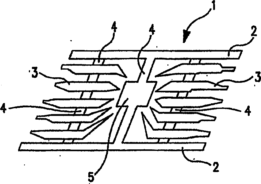
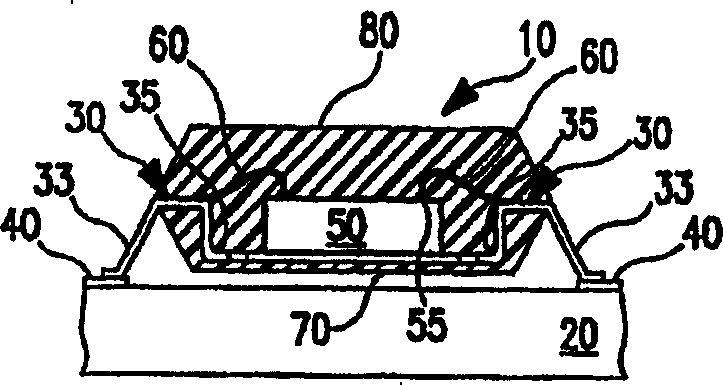
[0061] Figure 4-15band 16-24b show different embodiments for forming partially patterned leadframes that can have higher lead counts than close chip scale packages (CSPs). The method of the invention improves the automation of the production line and the quality and reliability of the packages produced thereby. This is accomplished by performing most of the manufacturing process steps and then partially patterning one side of the metal film to form a mesh lead frame. Compared with the conventional through-stencil type lead frame, the lead frame used in the present invention is partially patterned on one side and solid and flat on the other side. This structure improves mechanical and thermal performance so that it can be performed without distortion or deformation during chip bonding, wire bonding, and packaging. After the die-attach and wire-bond process steps are complete and the die and wire-bonds are bonded together and hermetically encapsulated in the molding compound,...


PUM

PropertyMeasurementUnit
Thicknessaaaaaaaaaa

Abstract

A method of making a lead frame and a partially patterned lead frame package with near-chip scale packaging (CSP) lead-counts is accomplished by performing a major portion of the manufacturing process steps with a partially patterned strip of metal formed into a web-like lead frame on one side, so that the web-like lead frame, which is solid and flat on the other side is also rigid mechanically and robust thermally to perform without distortion or deformation during the chip-attach and wire bond processes, both at the chip level and the package level. The bottom side of the metal lead frame is patterned to isolate the chip-pad and the wire bond contacts only after the front side, including the chip and wires, is hermetically sealed with an encapsulant. The resultant package being electrically isolated enables strip testing and reliable singulation without having to cut into any additional metal.

Description

field of invention [0001] The present invention relates generally to electronic packaging, and more particularly to partially patterned leadframes and methods of producing and using the same. Partially patterned lead frames are stronger and more stable than conventional lead frames. The robustness of the locally patterned leadframe improves the process of manufacturing the leadframe package and increases the overall reliability of the end product. Background technique [0002] In the production of electronic packages that use leadframes, there are several steps that subject the leadframes to mechanical and thermal stress. The thinner geometries of current leadframes and the ever increasing integration of integrated circuits on semiconductor chips have resulted in a process that places greater stress on the leadframe. Finer leadframes are much like delicate inserts or like carved metal structures that can be easily bent, broken, damaged or deformed (see Figures 1a and 1b). ...

Claims


Application Information

Patent Timeline
IPC IPC(8): H01L21/68H01L21/48H01L23/31H01L23/495H01L23/12H01L21/44H01L21/50H01L21/56H01L23/28H01L23/50
CPCH01L2924/01015H01L2224/85205H01L2924/01023H01L2224/45124H01L23/3114H01L2924/01046H01L2924/0105H01L2924/01082H01L2224/97H01L2224/32245H01L2924/01002H01L2224/16H01L2924/01029H01L21/4842H01L2924/00013H01L2224/13099H01L2924/01028H01L2224/48091H01L2224/16245H01L2224/49171H01L2924/014H01L2924/01013H01L2924/18301H01L2224/45147H01L2224/92247H01L24/97H01L24/45H01L2924/01047H01L2224/1134H01L2924/01079H01L24/48H01L2224/48247H01L2924/14H01L23/49548H01L2924/01033H01L2924/01005H01L2924/01006H01L24/49H01L2924/01078H01L2924/01057H01L2924/01075H01L2224/73265H01L21/561H01L21/4832H01L24/73H01L2224/45015H01L2924/12042H01L2924/181H01L2924/351H01L2924/00014H01L2224/85H01L2224/83H01L2224/81H01L2924/00012H01L2924/00H01L21/48H01L21/68H01L23/31H01L23/495
Inventor S·伊斯兰R·S·圣安东尼奥
Owner UNISEM MAURITIUS HLDG
Why Eureka
Try Eureka