
Film stretching loading device under scanning microscopy environment and film distortion measurement method

A loading device and scanning microscope technology, applied in scanning probe microscopy, measuring devices, scanning probe technology, etc., can solve the problem of whether the calibration of the sample axis and the tensile axis cannot be determined, and the clamping and bonding are reliable Whether it is uncertain or not, the effective elongation is difficult to measure directly, etc.

Inactive Publication Date: 2006-02-08
TSINGHUA UNIV
View PDF0 Cites 38 Cited by
  • Summary
  • Abstract
  • Description
  • Claims
  • Application Information

AI Technical Summary

Problems solved by technology

However, in the test, there is uncertainty about whether the clamping and bonding are reliable, the possible micro-mechanical damage caused by the preparation and installation of the sample cannot be known during the test, and whether the alignment of the sample axis and the tensile axis cannot be determined. The length is usually very short, and its effective elongation when stretched is difficult to measure directly, etc.
In addition, most of the above-mentioned measurements are macro measurements or carried out under an optical microscope, which obviously cannot meet the current requirements for the detection of film mechanical properties in the micro-scale field.

Method used

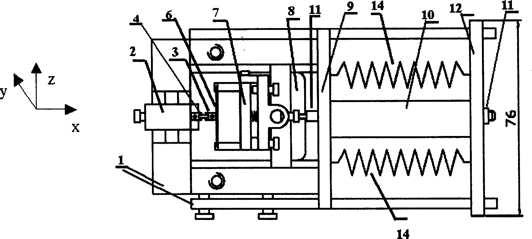

Image

  • Film stretching loading device under scanning microscopy environment and film distortion measurement method
  • Film stretching loading device under scanning microscopy environment and film distortion measurement method
  • Film stretching loading device under scanning microscopy environment and film distortion measurement method

Examples


Embodiment

[0089] Embodiment: The thin film tensile loading device under the atomic force scanning microscope environment is used for the tensile deformation detection of the iron-nickel thin film and the thin film tensile loading device under the electron beam scanning microscope environment is used for the tensile deformation detection of the pure gold film

[0090] Apply the two kinds of film detection stretching and loading devices developed by the present invention to quantitatively detect the deformation field of the film in the whole field or in a local area. The parameter selection is as follows: for the thin film tensile loading device under the environment of the atomic force scanning microscope, the system is driven by a piezoelectric ceramic micro-displacement device, the voltage resolution is 0.1V, the corresponding displacement accuracy is 0.0245 μm, and the displacement range is 42.6 μm. The beryllium bronze used The size of the force-measuring elastic beam is 20mm×2mm×0.09...


PUM


Abstract

The invention relates to a film-stretching loading device in scanning microscope environment and a film-deformation measuring method in the field of microscope scanning nondestructive inspection and precision machine. The device uses the designed mechanic structure, pressure ceramic driving system, force buffer system and so on which can do three-space location and angle adjustment to finish film deformation measuring on atom force scanning microscope and electron beam microscope detecting table. It can dose quantity detecting to deformation field of all region or localized region of the micro size film; the thickness of the detected film is from several micrometers to sub-micros; it can finish film original location and on line detecting under the high spacing resolution microscope atom force scanning microscope or electron beam scanning microscope environment combined with the double-exposure digital spot technique, the image related technique or micro-labeling technique.

Description

technical field [0001] The invention belongs to the fields of scanning microscopic non-destructive testing and precision machinery, and in particular relates to a film loading device in a scanning microscopic environment and a micro-area deformation detection method thereof. Background technique [0002] Thin-film materials and structures form the basis of microelectronic devices (MEMS) and micro-electro-optical devices (MEOS). Because MEMS devices require thin films not only to have good electrical, magnetic, and optical properties, but also require the thin film structure in the device to be able to withstand mechanical loads, transmit forces, and move. Obviously, as an integral part of micro-devices, thin-film structures will inevitably participate in the sensing, processing and execution functions of micro-devices. Therefore, any thin film failure due to environmental interaction will definitely affect the reliability of micro devices and structures. Studying the defor...

Claims


Application Information

Patent Timeline
IPC IPC(8): G01N3/28G01N3/00G01N19/00G01N13/16G01Q60/04
Inventor 李喜德杨燕
Owner TSINGHUA UNIV
Learn More