Method for removing lattice defect in pad area of semiconductor device

A lattice defect, semiconductor technology, applied in the direction of semiconductor devices, semiconductor/solid-state device manufacturing, semiconductor/solid-state device testing/measurement, etc., can solve the problems of DRAM reliability impact, not particularly reliable, lattice defects in the pad area, etc.

Inactive Publication Date: 2006-01-25
SEMICON MFG INT (SHANGHAI) CORP +1
View PDF0 Cites 11 Cited by
  • Summary
  • Abstract
  • Description
  • Claims
  • Application Information

AI Technical Summary

Problems solved by technology

However, this method of limiting the interval time (Q time) between the aluminum alloy passivation layer forming step (step 6) and the polyimide protective layer forming step (step 7) is not particularly reliable, once the Q time is exceeded , lattice defects will be generated in the pad area
Moreover, lattice defects were found in the pad area even after the polyimide protective layer was formed
These defects can negatively affect the reliability of DRAM

Method used


Image

  • Method for removing lattice defect in pad area of semiconductor device
  • Method for removing lattice defect in pad area of semiconductor device
  • Method for removing lattice defect in pad area of semiconductor device

Examples


specific Embodiment

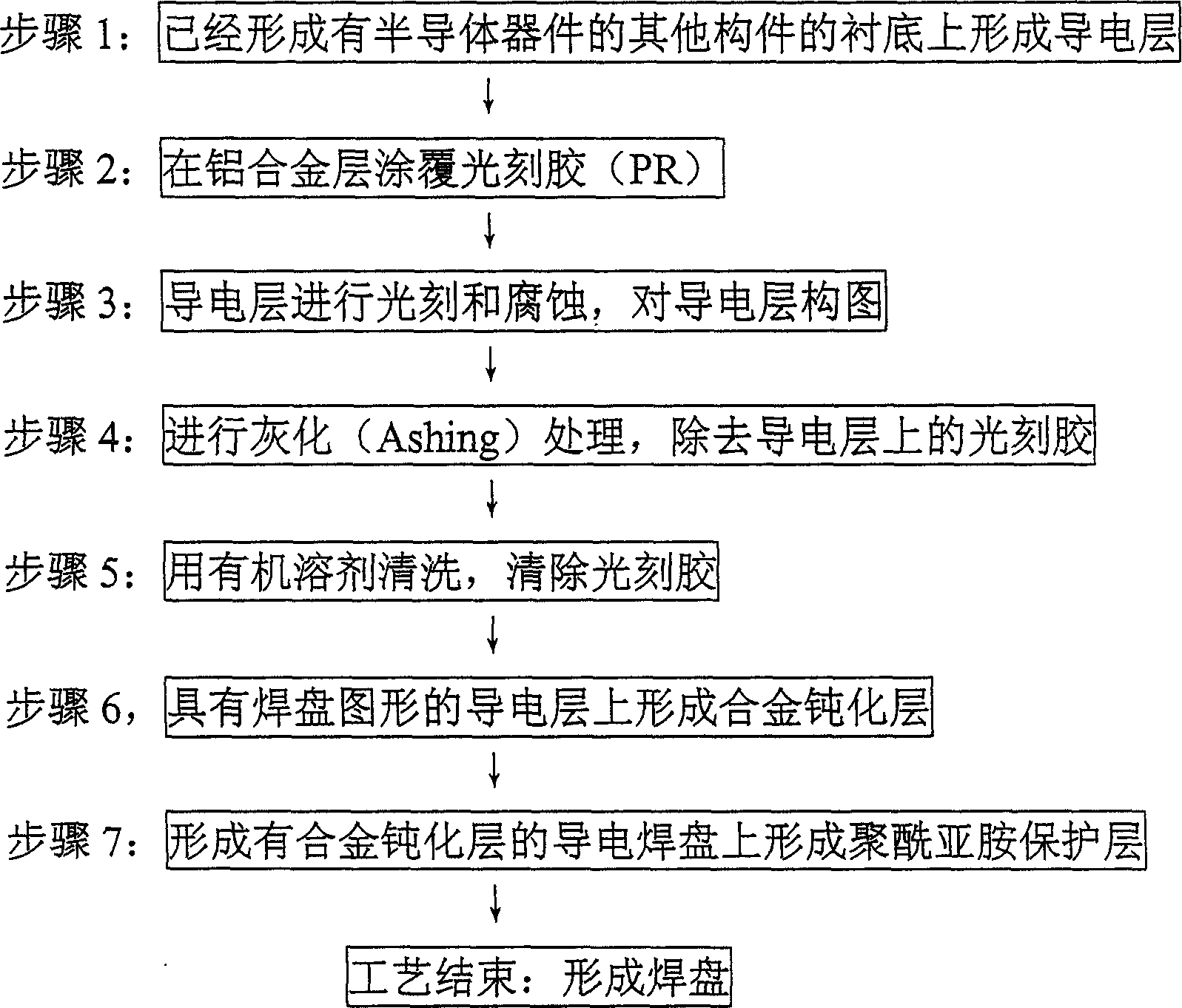
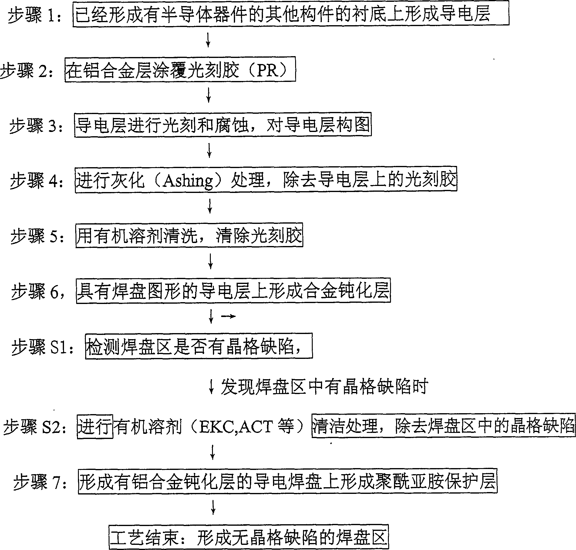
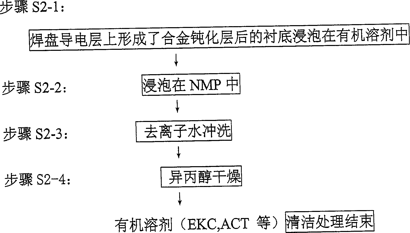
[0015] see below figure 2 and image 3 A method for cleaning and removing lattice defects in a pad (PAD) region of a semiconductor device with an organic solvent (EKC, ACT, etc.) according to the present invention will be described in detail. figure 2 It is a flow chart of the bonding pad formation process of the semiconductor device according to the present invention. image 3 It is a flow chart of organic solvent (EKC, ACT, etc.) cleaning treatment.

[0016] exist figure 2 The pad formation process flow of the semiconductor device according to the present invention is shown in figure 1 Step S1 (detecting whether there is a lattice defect in the pad area) is added between step 6 and step 7 of the pad formation process flow of the existing semiconductor device shown; and step S2 (when step S1 detects pad When there are lattice defects in the region, perform organic solvent (EKC, ACT, etc.) cleaning treatment). In step S1, use an optical microscope (OM) to detect whethe...


PUM


Abstract

This invention discloses a method for removing lattice defect in the pad zone, after forming an Al alloy purification layer and before forming a polyimide protection layer on the pad, it is tested that if the lattice defect exists in the pad, if so, the organic solvent of EKC and ACT cleaning process is made to remove the lattice defect in the zone.

Description

technical field [0001] The present invention relates to the method for removing the lattice defect in the bonding pad (PAD) region of semiconductor device, particularly relate to the method for cleaning and removing the lattice defect in the bonding pad (PAD) region of semiconductor device with organic solvent (EKC, ACT etc.) , especially a method for cleaning and removing lattice defects in a pad (PAD) region of a dynamic random access memory (hereinafter referred to as DRAM) with an organic solvent (EKC, ACT, etc.). Background technique [0002] Semiconductor devices include various types of active devices. For example, dynamic random access memory (DRAM) is a semiconductor device with a multi-layer structure. In order to connect components formed in various film layers together to form a complete DRAM, and the required electronic circuit modules are formed by connecting DRAM with other semiconductor devices or other electronic components. To complete these connections, ma...

Claims


Application Information

Patent Timeline
IPC IPC(8): H01L21/44H01L21/28H01L21/768H01L21/60H01L21/321H01L21/66
Inventor 吴长明蒋晓钧徐立黄光瑜
Owner SEMICON MFG INT (SHANGHAI) CORP
Why Eureka
Try Eureka