Method for producing portable information storage device

A storage device and manufacturing method technology, applied in semiconductor/solid-state device manufacturing, electrical components, circuits, etc., can solve problems such as deformation, easy deformation, appearance defects, etc.

Inactive Publication Date: 2006-01-04
DATAFAB SYST
View PDF0 Cites 0 Cited by
  • Summary
  • Abstract
  • Description
  • Claims
  • Application Information

AI Technical Summary

Problems solved by technology

[0008] However, as shown in Figure 2, in terms of the manufacturing process of the above-mentioned USB disk, it is often found that the housing 8 will be deformed after the injection molding of the encapsulating body 9. The reason for this is that the housing 8 is bent on a single metal plate. After forming, its joint seam 84 is all designed on the top wall 81 or the bottom wall 82, and with regard to the contact area with the envelope 9, the top wall 81 or the bottom wall 82 is relatively other sidewalls 83 have a connection with the envelope. 9 Larger contact area means that when the encapsulation body 9 is ejected, the pressure on the top wall 81 or the bottom wall 82 is far greater than that on the other side walls 83, so once the seam 84 is arranged on the top wall 81 or the bottom wall 82, the integrity of the top wall 81 or the bottom wall 82 will be insufficient to withstand the high pressure of the material when the encapsulation body 9 is ejected. On the other hand, the circuit unit 7 and the housing 8 are not in close contact. However, there are many gaps, so when the outside of the casing 8 bears the high pressure of material injection, it can be said that there is no support inside. The above factors are combined, and the result is that after the injection of the envelope 9 is completed, the top wall 81 or the bottom wall 82 It is easy to deform at the joint 84, which not only causes defects in appearance, but also may damage the internal circuit unit 7, resulting in many defective products.

Method used


Image

  • Method for producing portable information storage device
  • Method for producing portable information storage device
  • Method for producing portable information storage device

Examples


Embodiment Construction

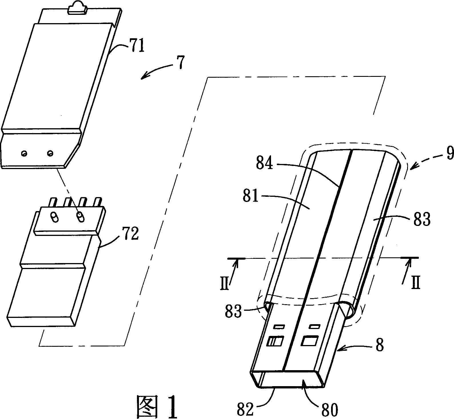
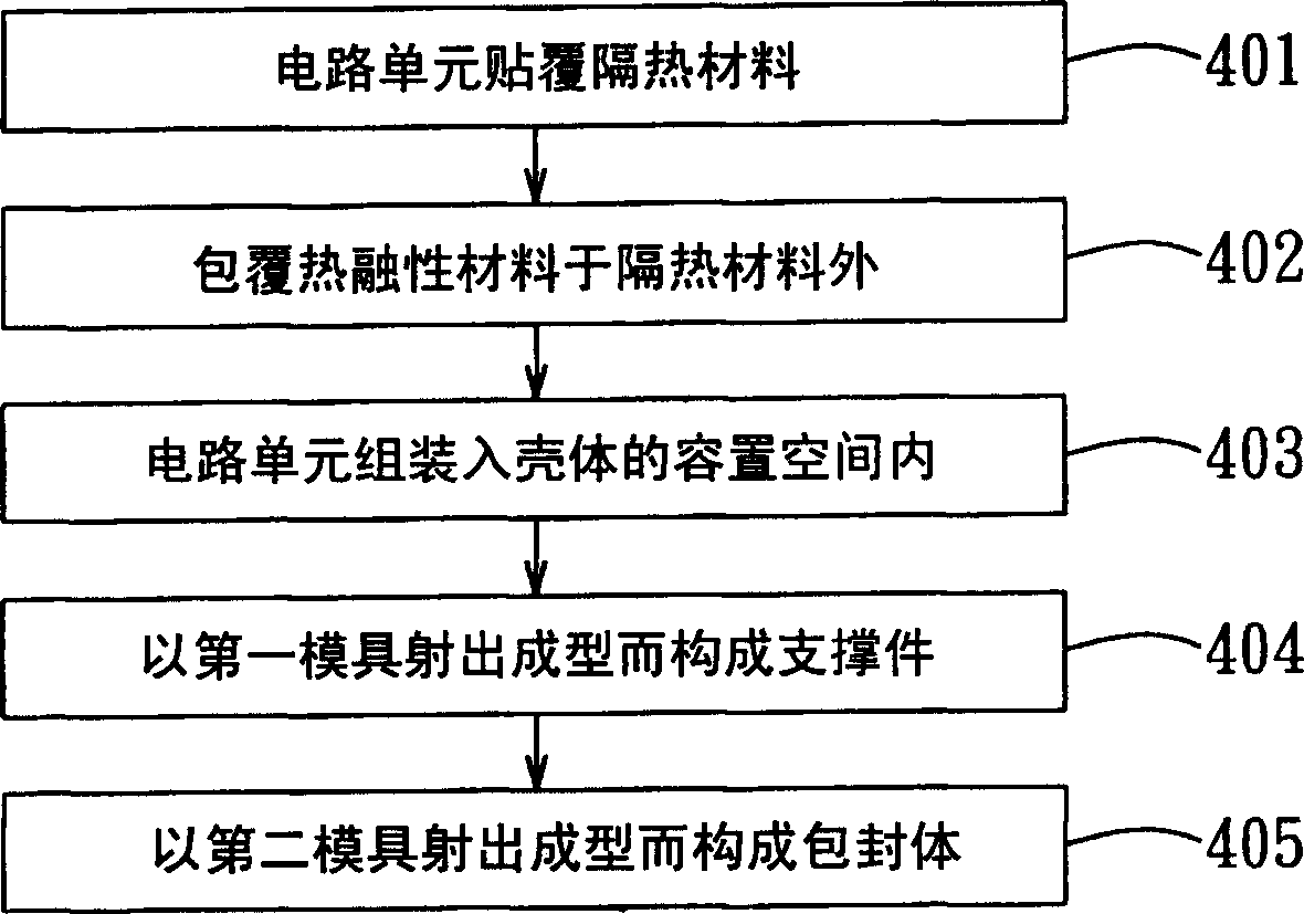
[0032] refer to image 3 A preferred embodiment of the manufacturing method of the portable information storage device of the present invention is applied to a USB disk.

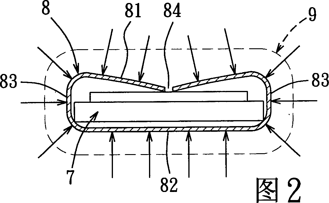
[0033] As shown in Fig. 4 and Fig. 5, the basic structure of the information storage device made by the present invention includes a circuit unit 1, a metal casing 2 and an encapsulating body 3 (described later) that is coated on the outside of the casing 2 by injection molding. ). The circuit unit 1 includes a circuit substrate 11 and an electrical connector 12 connected to the USB interface at the end of the circuit substrate 11, and the housing 2 is formed by stamping and bending a metal sheet, so that the interior constitutes a capacity enough to accommodate the circuit unit 1. The accommodating space 20 can be correspondingly divided into a body part 201 for accommodating the circuit board 11 and a plug-in part 202 for accommodating the electrical connector 12 in conjunction with the structure of the ci...


PUM


Abstract

This invention relates to a manufacturing method for a portable information storage device for manufacturing a portable information storage device containing a circuit unit, a metal shell and a package unit. The method includes taking a thermo material to adhere to the outside of the circuit unit, then putting the circuit unit in a containing space in the shell and positioning it in a die cavity formed by a first die set, filling the thermo material in the containing space of the shell to fill in the space between the circuit unit and the inside wall of the shell to make up of a support in the shell, finally, the assembly got at the previous step is positioned at the die cavity formed by a second die set to enable the thermo material to form a package body covering the shell.

Description

【Technical field】 [0001] The invention relates to a manufacturing method of a portable information storage device, in particular to a manufacturing method of a portable information storage device using flash memory (Flash Memory) as a main storage component. 【Background technique】 [0002] It is known that flash memory can be used to store electronic digital information. It will not disappear the stored electronic information in the state of no power supply. In addition, the mature integrated circuit manufacturing process makes the volume more miniaturized and other characteristics. It has been widely used. It is widely used in portable information storage devices commonly known as USB disks. [0003] As shown in FIG. 1 , it is a structure of a USB disk, which includes a circuit unit 7 , a metal shell 8 and an encapsulation 9 . [0004] The circuit unit 7 includes a circuit substrate 71 and an electrical connector 72 . The circuit substrate 71 is formed by welding a flash ...

Claims


Application Information

Patent Timeline
Patent Type & Authority Applications(China)
IPC IPC(8): H05K13/00H01L21/50
Inventor 林于荧
Owner DATAFAB SYST
Why Eureka
Try Eureka