Semiconductor device
A semiconductor and device technology, applied in the field of semiconductor devices, can solve the problem of low heating efficiency, achieve the effect of reducing cost, reducing cost, and preventing area increase
- Summary
- Abstract
- Description
- Claims
- Application Information
AI Technical Summary
Problems solved by technology
Method used
Image


Examples
no. 1 example
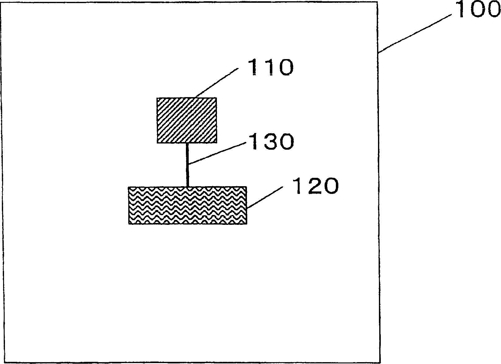
[0050] figure 1 is a block diagram showing the structure of a portion that detects temperature and performs heating in the semiconductor device according to the first embodiment of the present invention. exist figure 1 Among them, the semiconductor device 100 according to the embodiment includes a temperature sensor portion (temperature detection means) 110 , a heat generation portion (heat generation means) 120 , and control wiring 130 . The temperature sensor 110 and the heat generating part 120 are electrically connected to each other through the control wiring 130 .
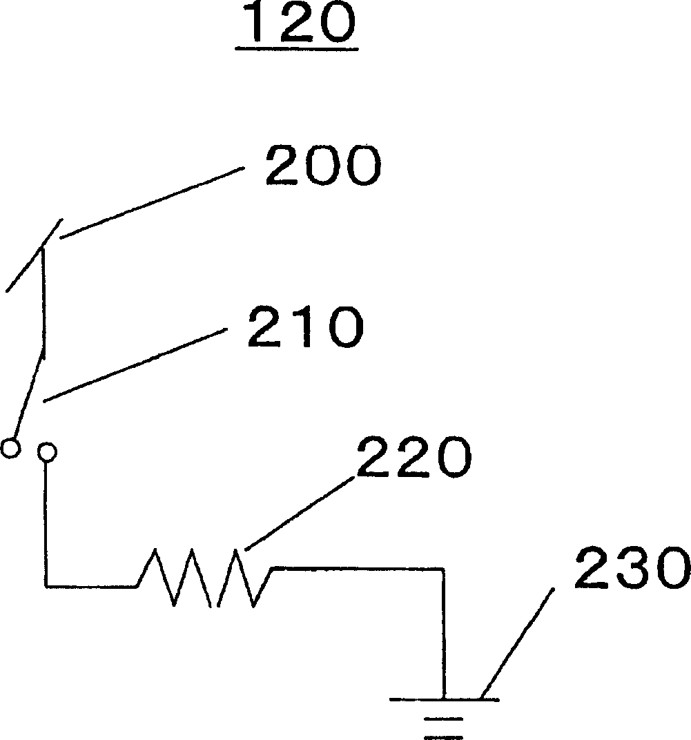
[0051] The temperature sensor section 110 includes a diode and a transistor having temperature characteristics, and outputs a heat generation instruction to the control wiring 130 when the temperature is equal to or lower than T degrees in normal operation of the semiconductor device 100, and outputs a heat generation instruction when the temperature is equal to or higher than T′ degrees. When (T′≧T), a n...
no. 2 example
[0060] Figure 7 is a block diagram showing the structure of a portion that detects temperature and performs heating in the semiconductor device according to the second embodiment of the present invention. exist Figure 7 Among them, the semiconductor device 100A according to this embodiment includes a plurality of heat generating sections 120 and is connected to the common temperature sensor section 110 . By providing the heat generating portion 120, the temperature sensor 110 can detect sudden cooling of the semiconductor device 100A, if any. Therefore, heating can be rapidly performed by the heat generating portion 120 so that the temperature of the semiconductor device 100A can be maintained constant or higher, and malfunction due to low temperature can be prevented.
no. 3 example
[0062] Figure 8 is a block diagram showing the structure of a portion that detects temperature and performs heating in a semiconductor device according to a third embodiment of the present invention. exist Figure 8 Among them, the semiconductor device 100B according to the present embodiment has a combination of a plurality of temperature sensor sections 110 and heat generating sections 120 connected thereto.
[0063] A combination of the temperature sensor 110 and the heat generating portion 120 is provided in the semiconductor device 100B. Even if a part of the semiconductor device 100B such as the local region 300 has a low temperature, therefore, the heat generating portion 120 in or near the local region 300 generates heat so that the semiconductor device 100B can be heated. Also, even if the temperature in the local area 300 rises under the heat generation of the heat generating portion 120, the temperature sensor portion 110 in or near the local area 300 detects the...
PUM
 Abstract
Description
Claims
Application Information
 - R&D
- Intellectual Property
- Life Sciences
- Materials
- Tech Scout
- Unparalleled Data Quality
- Higher Quality Content
- 60% Fewer Hallucinations
Browse by: Latest US Patents, China's latest patents, Technical Efficacy Thesaurus, Application Domain, Technology Topic, Popular Technical Reports.
© 2025 PatSnap. All rights reserved.Legal|Privacy policy|Modern Slavery Act Transparency Statement|Sitemap|About US| Contact US: help@patsnap.com