


Quick Research
Generate reliable direction feasibility study reports for your R&D in just a few steps.

Technical Q&A
Discover and master advanced knowledge NOW. Basics, ideas, possibilities, all at once.

Find Solutions
As an expert in R&D theories, this can generate solutions to your technical problems instantly.

Evaluate Feasibility
Analyze your overall solution with one click, know your potential R&D risks in advance.

Monitor Landscape
Get weekly tech updates, stay abreast of the latest tech innovations and key insights.
Method for implanting ions in semiconductor device
An ion implantation, semiconductor technology, applied in semiconductor/solid-state device manufacturing, instruments, table utensils, etc., can solve problems such as differences in electronic characteristics
- Summary
- Abstract
- Description
- Claims
- Application Information
AI Technical Summary
Problems solved by technology
Method used
Image

Examples
Embodiment Construction
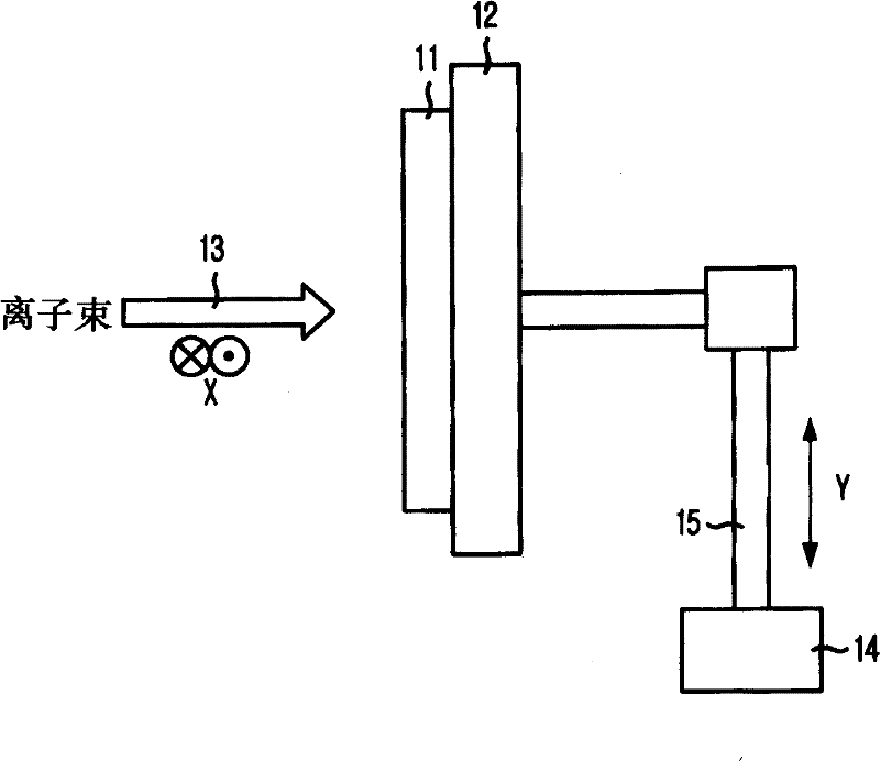
[0031] The ion implantation method in the semiconductor device according to the first embodiment of the present invention will be described in detail with reference to the accompanying drawings.
[0032] According to the present invention, the reciprocating scanning speeds in the X and Y directions are set differently according to the position of the substrate used in the non-uniform ion implantation method.
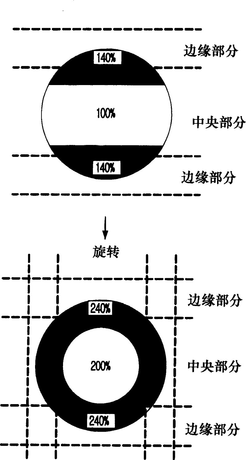
[0033] The present invention is invented based on the technical principle to identify the difference in the critical dimension (CD) of the gate in a substrate, and not cause the difference in the semiconductor device parameters in the substrate by performing non-uniform ion implantation.
[0034] For example, if the critical dimension of the gate in the central portion of the semiconductor is larger than in the edge portion of the substrate, the central portion of the semiconductor device will have a higher threshold voltage (V T ). Therefore, at the threshold voltage (...
PUM
 Abstract
Description
Claims
Application Information
 - R&D Engineer
- R&D Manager
- IP Professional
- Industry Leading Data Capabilities
- Powerful AI technology
- Patent DNA Extraction
Browse by: Latest US Patents, China's latest patents, Technical Efficacy Thesaurus, Application Domain, Technology Topic, Popular Technical Reports.
© 2024 PatSnap. All rights reserved.Legal|Privacy policy|Modern Slavery Act Transparency Statement|Sitemap|About US| Contact US: help@patsnap.com