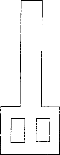
Thermal driven mini-type actuator
A micro-actuator and heat-driven technology, which is applied in the direction of microstructure technology, microstructure devices, and manufacturing microstructure devices, can solve the problems of killing cells and limiting cell operation, and achieves a structure that is not easy to break and has a low Young's modulus. Effect
- Summary
- Abstract
- Description
- Claims
- Application Information
AI Technical Summary
Problems solved by technology
Method used
Image
Examples
Embodiment 1
[0031] Such as figure 1 As shown, the thermally driven micro-actuator of the present invention has the effect of electrothermal braking, and can be designed and processed to have multiple cantilever beam structures (fingers) to complete micro-operations such as cell capture and clamping. Each cantilever beam is installed on a silicon substrate and has a three-layer structure. Titanium and platinum are used as resistance heating materials, and titanium and platinum are placed between parylene C (a polymer material); that is, titanium and platinum are clamped by parylene C. The three-story structure constitutes a cantilever beam. This embodiment is 4 cantilevers (or fingers), see Figure 4 .
[0032] Among them: the resistance heating material can be a few-shaped structure or any shape (see figure 2 , 3 ).
[0033] The maximum working temperature of the thermally driven micro-actuator cantilever beam of the present invention is 70°C, and the voltage when it is fully bent i...
Embodiment 2
[0047] This embodiment is 2 cantilevers (or fingers, see Figure 8 ). Its processing technology differs from embodiment 1 in that:
[0048] Use 6100 Å light conditions to grow silicon oxide on the silicon chip as the substrate 1; apply a photoresist with a thickness of 1.0 μm on the desired part of the silicon substrate; the thickness of parylene C as the first layer 3 is 0.25; the resistance material titanium The thickness is 550 Å, and the platinum thickness is 1950 Å.
Embodiment 3
[0050] The present embodiment is 6 cantilever beams, and its processing technology differs from embodiment 1 in that:
[0051] On the silicon chip, use 5900 Å light conditions to grow silicon oxide as the substrate 1; apply a photoresist with a thickness of 1.8 μm on the required part of the silicon substrate; the thickness of parylene C as the first layer 3 is 0.35; the resistance material titanium The thickness is 450 Å, and the platinum thickness is 2050 Å.
[0052] The two usage states of the six-finger gripper in this embodiment are as follows: Figure 7-1 , 7-2shown. The index of the present invention should be determined according to the actual application.
PUM
| Property | Measurement | Unit |
|---|---|---|
| thickness | aaaaa | aaaaa |
| power consumption | aaaaa | aaaaa |
| thickness | aaaaa | aaaaa |
Abstract
Description
Claims
Application Information
 - Generate Ideas
- Intellectual Property
- Life Sciences
- Materials
- Tech Scout
- Unparalleled Data Quality
- Higher Quality Content
- 60% Fewer Hallucinations
Browse by: Latest US Patents, China's latest patents, Technical Efficacy Thesaurus, Application Domain, Technology Topic, Popular Technical Reports.
© 2025 PatSnap. All rights reserved.Legal|Privacy policy|Modern Slavery Act Transparency Statement|Sitemap|About US| Contact US: help@patsnap.com


