High matching low power consumption low noise CDS cirecuit structure

A technology with circuit structure and low power consumption, which can be used in improving amplifiers to reduce noise impact, TV, color TV, etc. It can solve the problems of system chip battery life reduction, increase of image sensor chip area, difficulty in obtaining readout rate, etc.

Inactive Publication Date: 2005-05-25
INST OF MICROELECTRONICS CHINESE ACAD OF SCI
View PDF0 Cites 2 Cited by
  • Summary
  • Abstract
  • Description
  • Claims
  • Application Information

AI Technical Summary

Problems solved by technology

[0004] The existing CDS circuit has several disadvantages: (1) a large number of NMOSFET tubes are used, which increases the chip area of ​​the image sensor; (2) a large number of column selection PMOSFET tube parasitic capacitances and a large number of parasitic capacitances of the output bus ar...

Method used


Image

  • High matching low power consumption low noise CDS cirecuit structure
  • High matching low power consumption low noise CDS cirecuit structure

Examples


Embodiment Construction

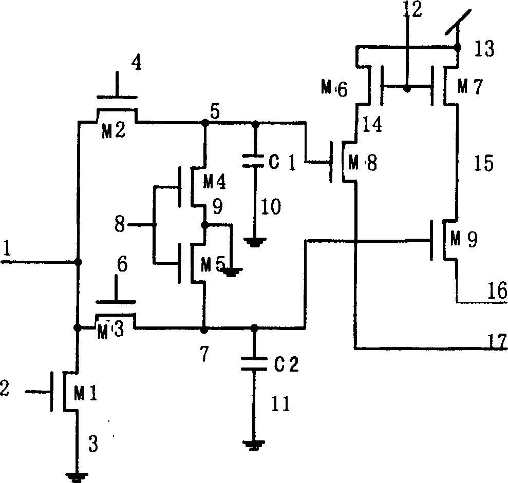
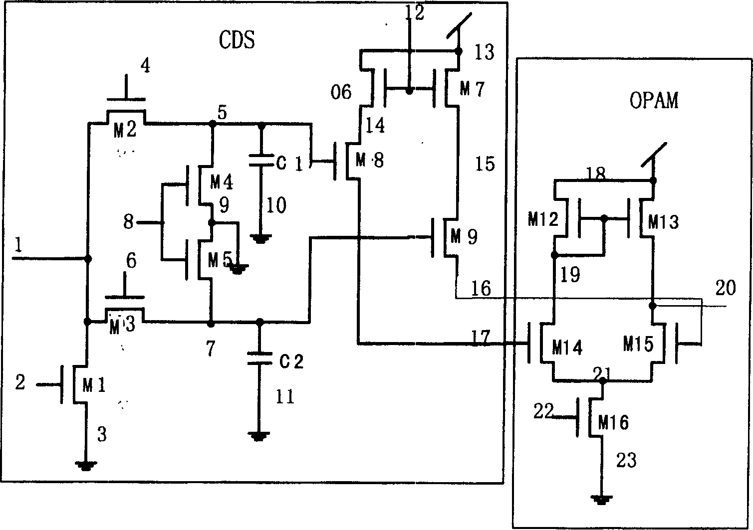
[0019] refer to figure 1 , figure 1 It is a schematic diagram of the circuit structure of the present invention. The present invention is a low-power correlated double-sampling circuit structure. This structure has the advantages of good matching, low power consumption, and low noise, including:

[0020] The proposed correlated double sampling circuit is composed of bias transistor M1, sampling switching transistors M2 and M3, sampling capacitors C1 and C2, snap transistors M4 and M5, column selection transistors M6 and M7, source follower transistors M8 and M9, two of them Sampling switch transistors M2 and M3 and column selection transistors M6 and M7 use P-type MOS transistors, and the rest use N-type MOS transistors. The source of the bias transistor M1 is grounded 3, the gate is connected to the bias voltage terminal 2, and the drain is connected to the input terminal 1; the drains of the two sampling switching transistors M2 and M3 are connected to the signal input term...


PUM


Abstract

A high matching low power dissipation low noise CDS circuit structure contains two sample switching transistors M2, M3, a array biasing transistor M1, two source connected transistors M4, M5, two capacitors C1, C2, a pair of array follow transistors M8, M9, a pair of source connected and grid connected array gate transistors M6, M7.

Description

technical field [0001] The invention belongs to the ultra-large-scale integrated circuit design in the field of microelectronics and solid-state electronics, and is a CDS circuit structure with high matching, low power consumption and low noise. Background technique [0002] The noise of the readout circuit mainly includes the inherent noise of the devices used in the readout circuit, and the additional noise introduced by the circuit structure and circuit working mode. The CMOS readout circuit only includes three components: a photodetector, a MOS tube, and a MOS capacitor, and the MOS capacitor is formed by a drain-source short circuit of the MOS tube. Therefore, photodetection devices and MOS tubes are the main noise sources of the readout circuit. These noises include: on the one hand, the inherent noise of photoelectric detection devices and MOS tubes, and on the other hand, caused by the structure and working mode of the readout circuit. These noises limit the dynami...

Claims


Application Information

Patent Timeline
IPC IPC(8): H03F1/00H03F1/08H03F1/26H03F3/45H04N5/30
Inventor 金湘亮陈杰仇玉林
Owner INST OF MICROELECTRONICS CHINESE ACAD OF SCI
Why Eureka
Try Eureka