Stacked semiconductor device and semiconductor chip control method

A semiconductor and chip technology, applied in the field of stacked semiconductor devices, can solve problems such as complex manufacturing process, increased manufacturing cost, and increased manufacturing steps

Inactive Publication Date: 2005-04-27
PS4 LUXCO SARL
View PDF2 Cites 17 Cited by
  • Summary
  • Abstract
  • Description
  • Claims
  • Application Information

AI Technical Summary

Problems solved by technology

This leads to an increase in manufacturing steps
[0025] On the other hand, a complex manufacturing process
Disadvantageously, this will lead to an increase in manufacturing cost

Method used


Image

  • Stacked semiconductor device and semiconductor chip control method
  • Stacked semiconductor device and semiconductor chip control method
  • Stacked semiconductor device and semiconductor chip control method

Examples


Embodiment Construction

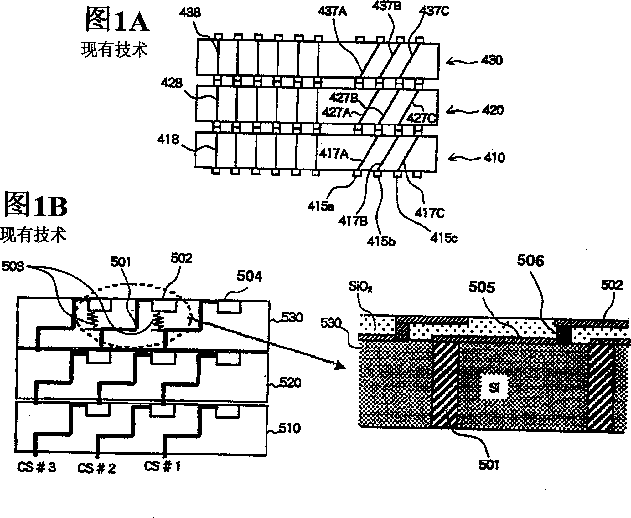
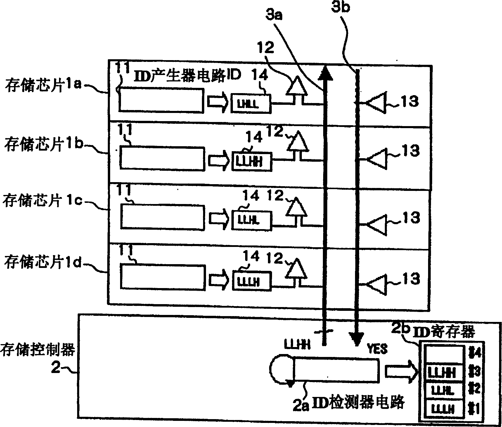
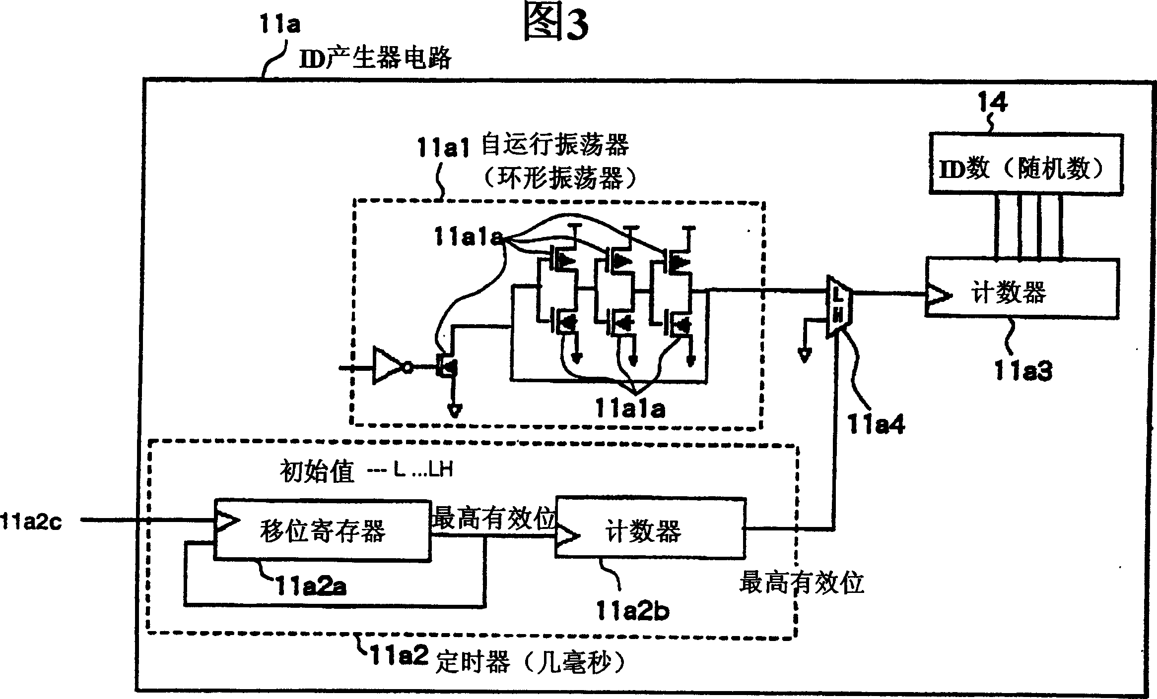
[0092] figure 2 is an explanatory diagram illustrating the basic configuration of a semiconductor memory device. figure 2 The illustrated semiconductor device is a typical semiconductor device according to one embodiment of the present invention. It should be noted that the semiconductor device is not limited to the semiconductor memory device, but may be appropriately changed.

[0093] exist figure 2 In this example, a semiconductor memory device includes memory chips 1a-1d, and a memory controller 2. The memory chips 1a-1d are examples of semiconductor chips. It should be noted again that the semiconductor chip is not limited to the memory chip but may be appropriately changed. The storage controller 2 is an example of a controller.

[0094] The memory chips 1a-1d are stacked one on top of the other. The number of memory chips is not limited to 4 but can be changed appropriately. Also, the memory chips 1 a - 1 d may or may not be laminated on the memory controller 2 ....


PUM


Abstract

Each of stacked memory chips has an ID generator circuit for generating identification information in accordance with its manufacturing process. Since the memory chip manufacturing process implies process variations, the IDs generated by the respective ID generator circuits are different from one another even though the ID generator circuits are identical in design. A memory controller instructs an ID detector circuit to detect the IDs of the respective memory chips, and individually controls the respective memory chips based on the detected IDs.

Description

technical field [0001] The present invention relates to a semiconductor device and a control method of a semiconductor chip, and more particularly to a stacked semiconductor device having semiconductor chips such as memory chips stacked one on top of another, and a method of controlling the semiconductor chip. Background technique [0002] It is foreseeable that if semiconductor manufacturing processes encounter difficulties in miniaturization in the future, increases in chip size associated with improvements in the functions of LSI chips (for example, increased storage capacity of DRAM) cannot be avoided by process-based miniaturization. [0003] In order to solve this possible problem, it is proposed that semiconductor devices (for example, DRAM) adopt a CoC (Chip on Chip) structure, which may include one layer stacked on another for the three-dimensional expansion function of the LSI chip (for example, the storage capacity of DRAM). An LSI chip on one. [0004] Currently...

Claims


Application Information

Patent Timeline
Patent Type & Authority Applications(China)
IPC IPC(8): G11C11/408G11C5/06G11C8/12G11C11/401G11C11/407G11C11/413H01L23/495H01L23/544H01L25/00H01L25/065H01L25/18
CPCH01L2924/0002H01L2225/06513H01L2225/06572H01L2924/15311H01L2924/15331H01L2223/5444H01L25/18H01L23/544H01L25/0657H01L2225/06527H01L2224/16
Inventor 船场诚司西尾洋二
Owner PS4 LUXCO SARL
Why Eureka
Try Eureka