Quasi-dual-gate field effect transistor

A field-effect transistor and gate-behind technology, applied in the field of microelectronic semiconductors, can solve the problems of large parasitic series resistance of FinFET, affecting large-scale integration of devices, serious hot electron effect, etc. The effect of the restriction on the width of the isolation area

Inactive Publication Date: 2005-03-23
PEKING UNIV
View PDF0 Cites 3 Cited by
  • Summary
  • Abstract
  • Description
  • Claims
  • Application Information

AI Technical Summary

Problems solved by technology

For FinFET, in order to effectively suppress its leakage current, the width of the isolation region (fin) must be continuously reduced, but if the width of fin is very small, the parasitic series resistance of FinFET will be very large, and its drive current will be lost
For example, for a 10nm FinFET, in order to suppress its leakage current, the width of its fin cannot be greater than 5nm, which is difficult to achieve in terms of technology
Moreover, as the size of the device decreases, the hot electron effect of the device becomes more and more serious, and the reliability problem of the gate oxide becomes more and more serious, which affects the large-scale integration of the device.

Method used


Image

  • Quasi-dual-gate field effect transistor
  • Quasi-dual-gate field effect transistor
  • Quasi-dual-gate field effect transistor

Examples


Embodiment Construction

[0019] Specific implementation examples

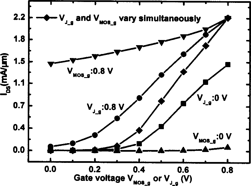
[0020] reference figure 2 , The quasi-dual gate field effect transistor of the present invention includes a source region 3, a drain region 3, an isolation region 6, a body 4, a front gate 1 and a rear gate 5, and an isolation region 6 is provided between the source and drain regions 3 and the body 4. The front gate 1 is polysilicon, a layer of gate oxide 2 is provided between the front gate 1 and the body 4, the back gate 5 is doped monocrystalline silicon, and the back gate 5 and the body 4 are directly connected to form a PN junction. Due to the connection between the rear gate and the body, the width of the body can be controlled within the range of 3 / 5 to 1 of the length of the front and rear gates, and the width of the isolation region can also be 2 to 4 times the length of the front and rear gates. The length can be controlled to be 1 to 1.5 times the length of the front and rear grids.

[0021] The design parameters of the present...


PUM


Abstract

The invention provides a quasi dual junction grid field effect transistor and belongs to the field of the micro-electronic semiconductor technology. The quasi dual junction grid field effect transistor includes the source, drain region, isolation region, body, front grid and back grid. The front grid is the multi crystalline silicon and there is a layer of grid oxygen between the front grid and the channel region. The back grid is the adulterated single crystal of silicon and connects with the body directly to form the P-N junction. Compared with the traditional FinFET, the structure of the invention has two different types of control grids. The back grid (P-N junction gate) is used to exhaust the channel region and to restrain the leakance, while the front grid is used to make the inversion layer in the channel region and to produce great drive current. That the back grid and the front grid of the invention connect with each other directly increases the grid control power of the device greatly and dulls the restrain to the breadth of the isolation region.

Description

Technical field [0001] The invention belongs to the technical field of microelectronic semiconductors, and specifically relates to a quasi-double-gate field effect transistor. Background technique [0002] With the continuous shrinking of the device size, the leakage current of the device has become the main obstacle to the shrinking of the device. In recent decades, scientific researchers have continuously proposed new technologies and device structures, such as SOI (Silicon-on-Insulator) technology, dual-gate devices, tri-gate devices, Ω-gate devices, and even wrap-gate devices. The purpose is to reduce the leakage current of the device and enhance the gate control capability of the device. After several years of development, dual-gate devices have gradually come to the fore and are generally considered by the scientific community to be one of the devices most likely to be applied in the industry. Double-gate devices have very perfect electrical characteristics, such as small l...

Claims


Application Information

Patent Timeline
Patent Type & Authority Applications(China)
IPC IPC(8): H01L29/772
CPCH01L29/785H01L29/7832
Inventor 陈刚黄如张兴王阳元
Owner PEKING UNIV
Why Eureka
Try Eureka