Electrode piece for electrostatic chuck, electrostatic chuck device and its adsorptiong method
An electrostatic chuck and electrode sheet technology, applied in the field of electrode sheets, can solve the problems of increased leakage current between electrodes, foreign matter in the binder, and reduced insulation resistance value, etc., and achieves strong adsorption force, high utilization value, and durability. high effect
- Summary
- Abstract
- Description
- Claims
- Application Information
AI Technical Summary
Problems solved by technology
Method used
Image
Examples
Embodiment 1
[0042] Embodiment 1 (making of electrostatic chuck device)
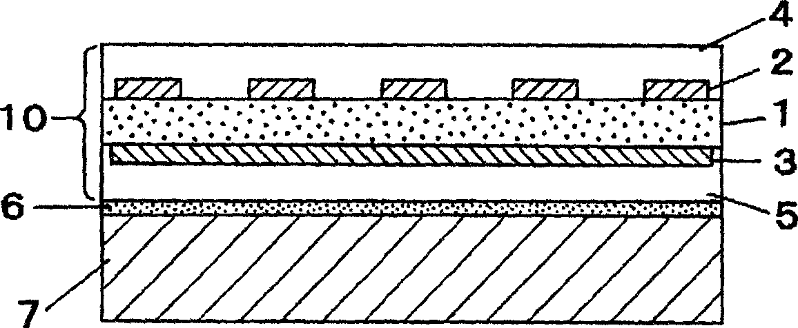
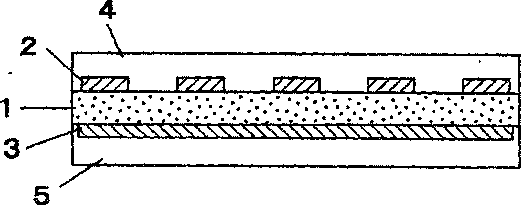
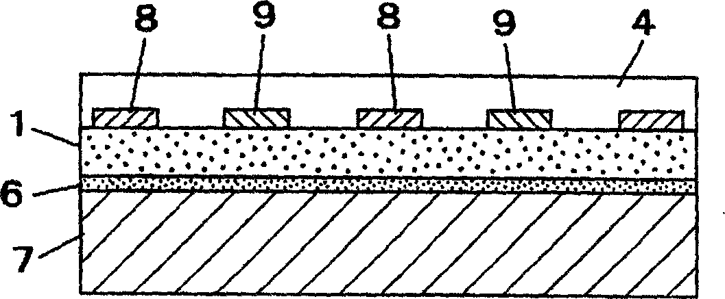
[0043] Copper foil with a thickness of 12 μm (manufactured by Mitsui Metal Mining Co., Ltd., trade name: TQ) is laminated on both sides of a polyimide film (manufactured by Toray Dupont Co., Ltd., trade name: Capton 200H, thickness 50 μm) through a 20 μm thick adhesive film. -VLP). Next, by etching, the first electrode layer ( Figure 4 The shape shown), the first electrode layer is composed of a comb-shaped electrode with a width of 5 mm and a width of 5 mm insulated parts alternately arranged, with an area of 90 × 90 mm; The second electrode layer ( Figure 5 After that, on the two electrode layers, a polyimide film (Capton 200H) was laminated through a 20 μm adhesive film to obtain an electrode sheet.
[0044] After cutting the electrode sheet to a predetermined size, the second electrode layer side was bonded to a 5×100×100 mm aluminum base using a 20 μm thick adhesive film to produce an electrostatic chuck ...
Embodiment 2
[0049] An electrostatic chuck device was produced with the same materials and operating conditions as in Example 1, except that the comb-shaped design of the first electrode layer was changed to a width of 2 mm for the conductive part and 2 mm for the width of the insulating part.
Embodiment 3
[0051] An electrostatic chuck device was produced with the same materials and operating conditions as in Example 1, except that the comb-shaped design of the first electrode layer was changed to a width of 10 mm for the conductive part and 10 mm for the width of the insulating part.
PUM
 Abstract
Description
Claims
Application Information
 - R&D Engineer
- R&D Manager
- IP Professional
- Industry Leading Data Capabilities
- Powerful AI technology
- Patent DNA Extraction
Browse by: Latest US Patents, China's latest patents, Technical Efficacy Thesaurus, Application Domain, Technology Topic, Popular Technical Reports.
© 2024 PatSnap. All rights reserved.Legal|Privacy policy|Modern Slavery Act Transparency Statement|Sitemap|About US| Contact US: help@patsnap.com


