Interlayer connection structure and its building method

A technology of interlayer connection and conductive connection, which is applied in the direction of electrical connection formation of printed components, multi-layer circuit manufacturing, electrical components, etc. It can solve the problems of difficult uniform contact, inability to conduct conductive connection, and reinforcing fiber hindering contact, etc., to achieve uniform thickness Effect

Inactive Publication Date: 2005-01-12
DENKA CO LTD
View PDF3 Cites 9 Cited by
  • Summary
  • Abstract
  • Description
  • Claims
  • Application Information

AI Technical Summary

Problems solved by technology

[0008] However, in the conductive connection structure formed in this way, the metal protrusions and the copper foil are only crimped. In addition, resin is easily mixed between the two, and it is difficult to make uniform contact between the surfaces. It cannot be said that the conductive connection between the wiring layers is reliable. high reliability
In particular, in the case where the insulating layer contains reinforcing fibers, the reinforcing fibers prevent contact and cannot be electrically connected

Method used


Image

  • Interlayer connection structure and its building method
  • Interlayer connection structure and its building method
  • Interlayer connection structure and its building method

Examples


Embodiment Construction

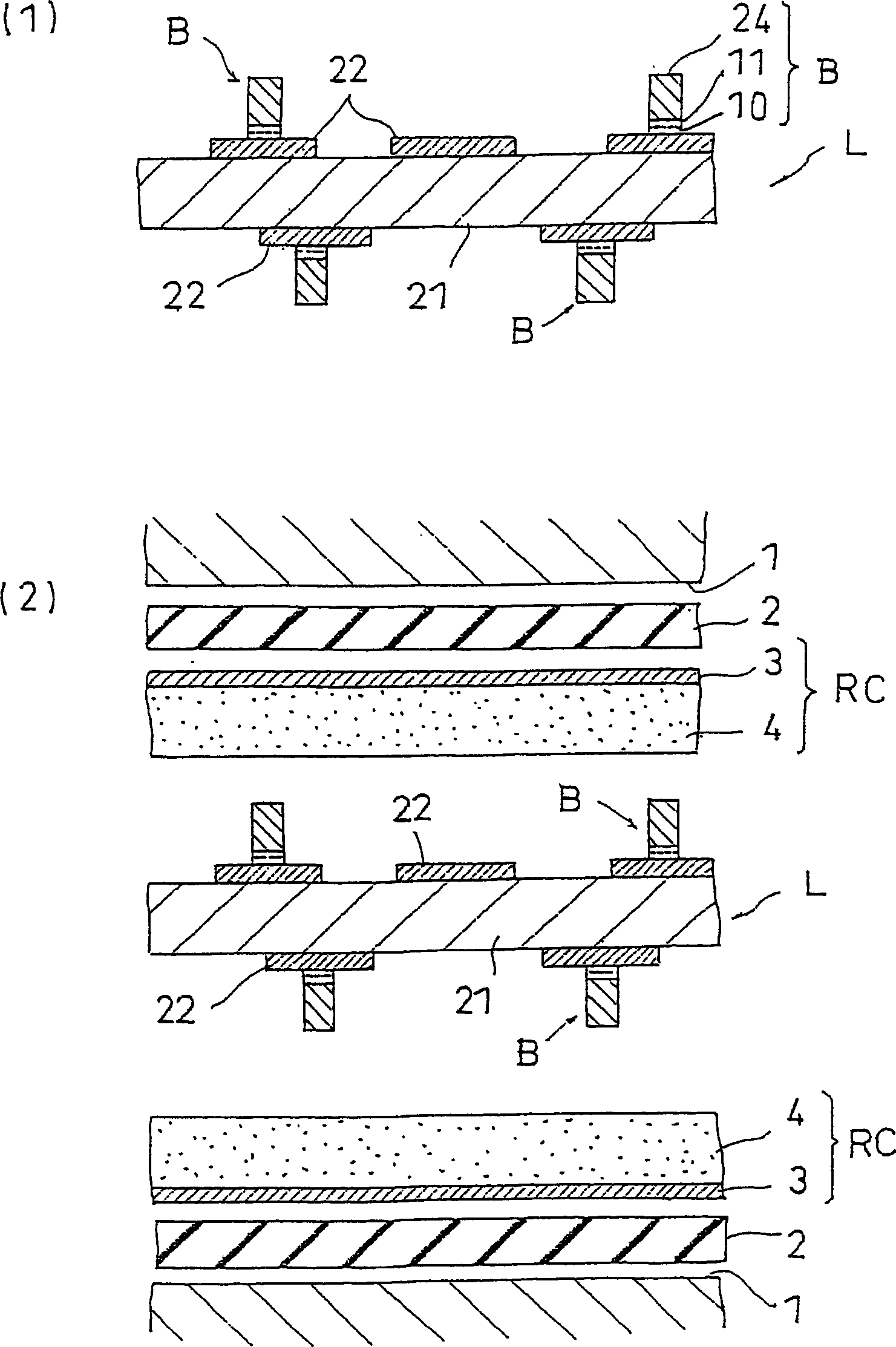
[0025] (The first method of forming an interlayer connection structure invented)

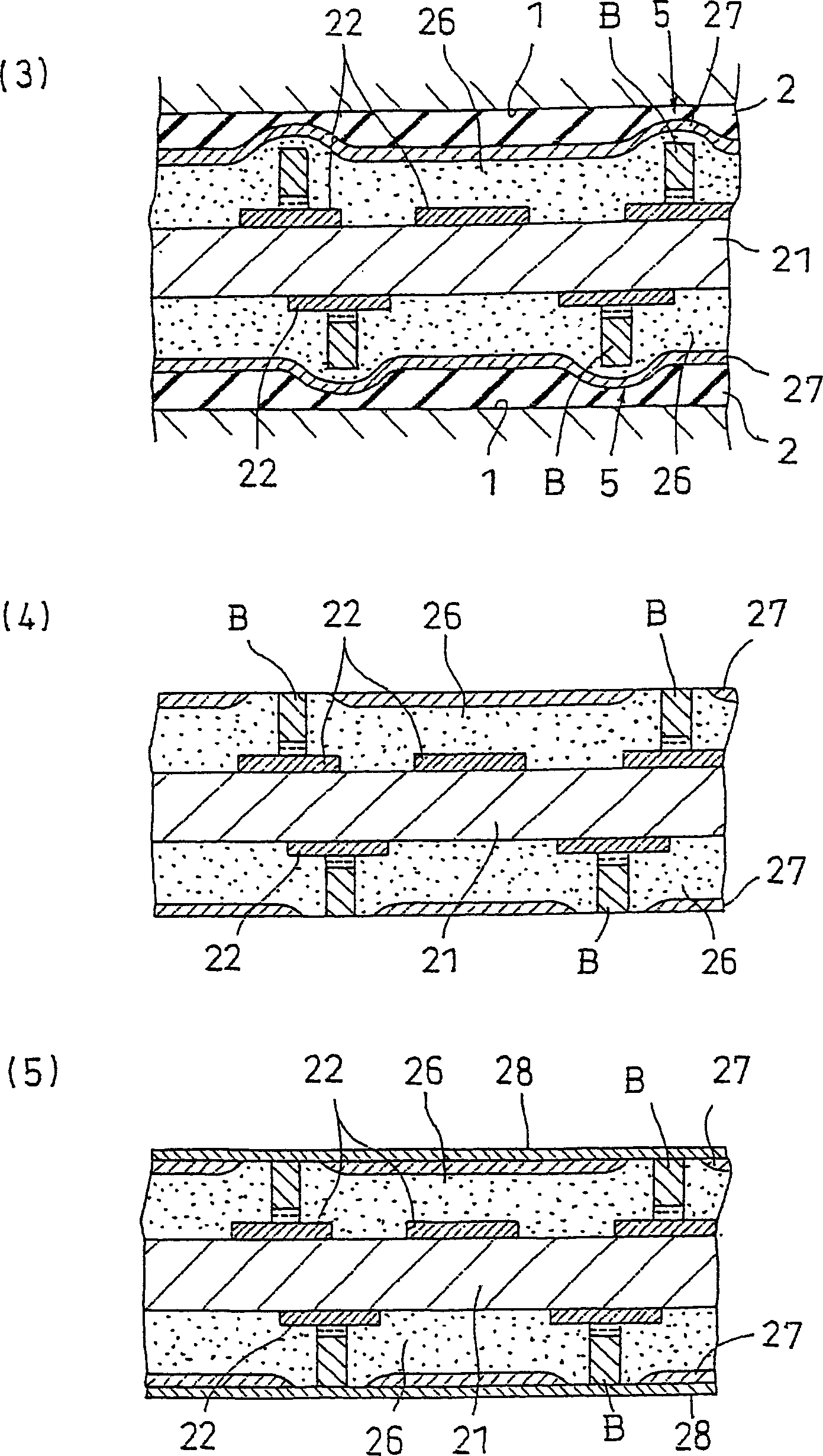
[0026] In this embodiment, it is described that the wiring layer 22 formed on both sides of the central substrate and the metal layer 27 formed on the upper layer via the insulating layer 26 are connected between layers through the interlayer connection protrusion B to form an interlayer connection structure. example of.

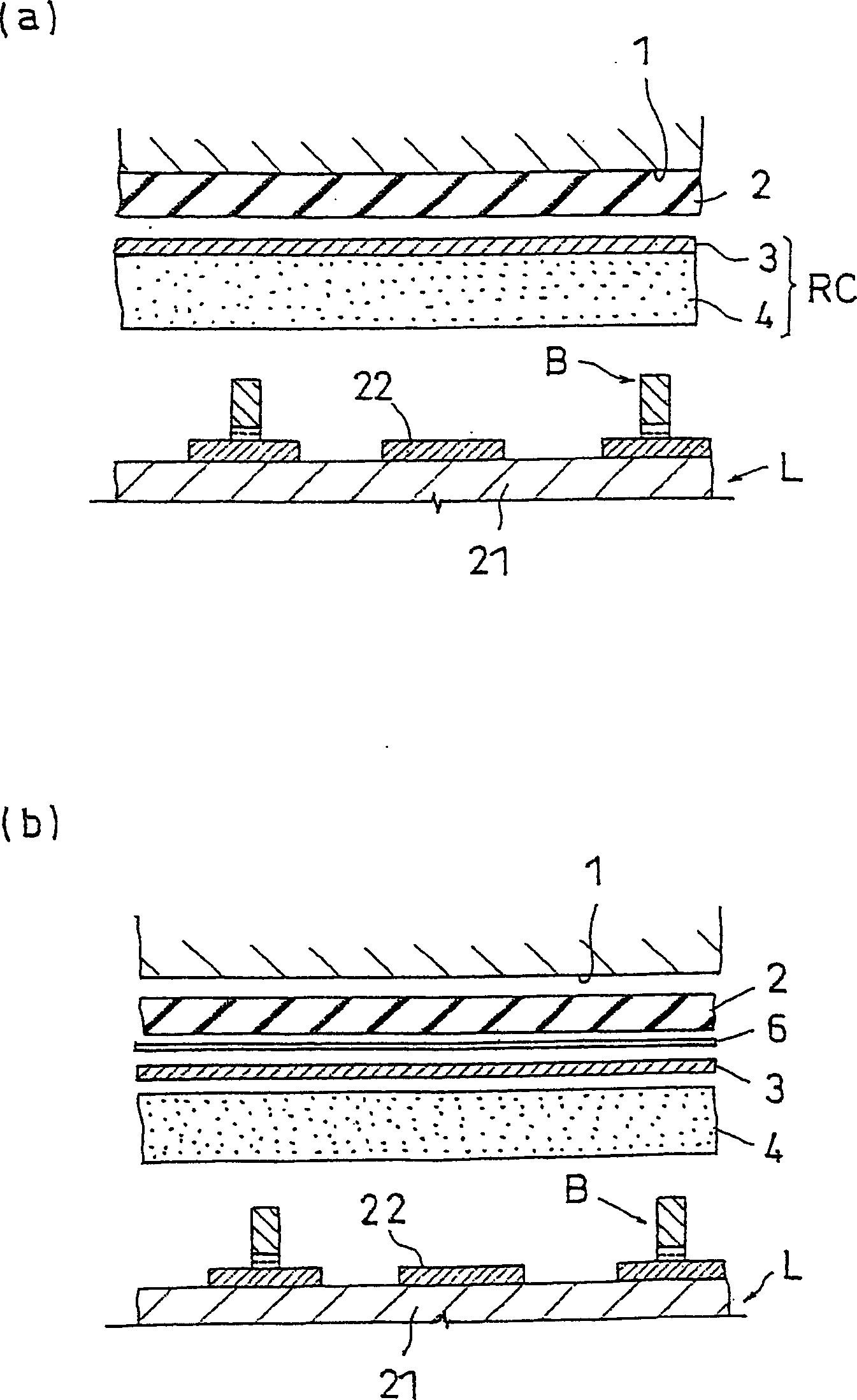
[0027] First, if figure 1 As shown in (1), a laminated body L is prepared in which the pattern of the wiring layer 22 is formed on both surfaces of the base material 21 and the interlayer connection protrusions B are formed on the wiring layer 22 . At this time, any method can be used for patterning the wiring layer 22, for example, a method using an etching resist, a method using a resist for pattern plating, or the like can be used. As the metal constituting the wiring layer 22, copper, nickel, tin, etc. are generally used, and copper is preferably used. As the base mate...


PUM


Abstract

A method for building an interlayer connection structure where wiring layers (22) or metallic layers (27) formed on both sides of an insulating layer (26) are interlayer-connected through an interlayer connection projection (B), comprising the steps of stacking at least a sheet member (2) deformable concavely, a metallic layer forming member, and a thermally-adhesive insulating layer forming member in this order of mention between a press surface (1) and a body to be laminated and having the interlayer connection projection, conducting hot press of the stack using the press surface to produce a laminate having a projection in a position corresponding to the interlayer connection projection and having a metallic layer on its surface, removing the projection of the laminate to expose the interlayer connection projection, and electrically connecting the exposed interlayer connection projection and the metallic layer disposed near the interlayer connection projection with the insulating layer interposed therebetween, whereby the thickness of the insulating layer between layers can be uniformed, and the planarization of the surface and thickness control of the insulating layer can be effected even if the insulating layer contains reinforcing fibers. An interlayer connection structure built by the method and a multilayer wiring board are also disclosed.

Description

technical field [0001] The present invention relates to a method for forming an interlayer connection structure for forming a conductive connection structure between wiring layers or an interlayer heat dissipation structure on a multilayer wiring substrate, as well as an interlayer connection structure formed by the method and a multilayer wiring substrate . Background technique [0002] In recent years, along with miniaturization and higher functionality of electronic devices, there have been increasing demands for multilayer, thinner layers, and miniaturized patterns on wiring boards on which electronic components are mounted. Therefore, the insulating layer or wiring layer constituting the multilayer wiring board also tends to be thinned. In addition, in the case of controlling the characteristic impedance corresponding to a high-frequency signal, it is necessary to control the thickness of the insulating layer or the wiring layer with high precision. [0003] When manu...

Claims


Application Information

Patent Timeline
Patent Type & Authority Applications(China)
IPC IPC(8): H05K3/46
CPCH05K2203/025H05K3/4647H05K2203/068H05K2201/0347H05K2201/091H05K3/4652H05K3/46
Inventor 吉村荣二北村充彦巢山育男
Owner DENKA CO LTD
Why Eureka
Try Eureka