
Adulterating method used for adulterating vertical pulling silicon mono crystal and its adulterating funnel

A technology of Czochralski silicon single crystal and funnel, which is applied in the direction of single crystal growth, single crystal growth, chemical instruments and methods, etc., can solve the problems of difficult crystal growth, complicated high-concentration uniform doping technology, etc. The effect of reducing environmental pollution

Active Publication Date: 2004-12-22
金瑞泓科技(衢州)有限公司
View PDF0 Cites 21 Cited by
  • Summary
  • Abstract
  • Description
  • Claims
  • Application Information

AI Technical Summary

Problems solved by technology

In fact, crystal growth is very difficult when the concentration is close to the limit value. One of the difficulties is that the high-concentration uniform doping technology is more complicated

Method used


Image

  • Adulterating method used for adulterating vertical pulling silicon mono crystal and its adulterating funnel
  • Adulterating method used for adulterating vertical pulling silicon mono crystal and its adulterating funnel
  • Adulterating method used for adulterating vertical pulling silicon mono crystal and its adulterating funnel

Examples


Embodiment Construction

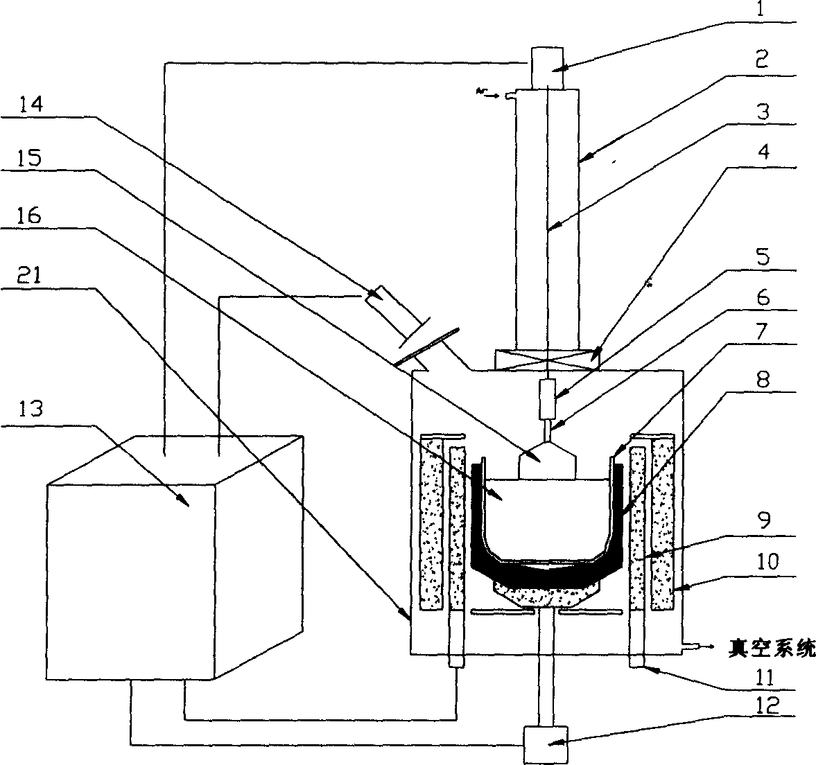
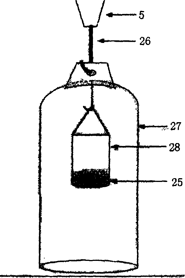
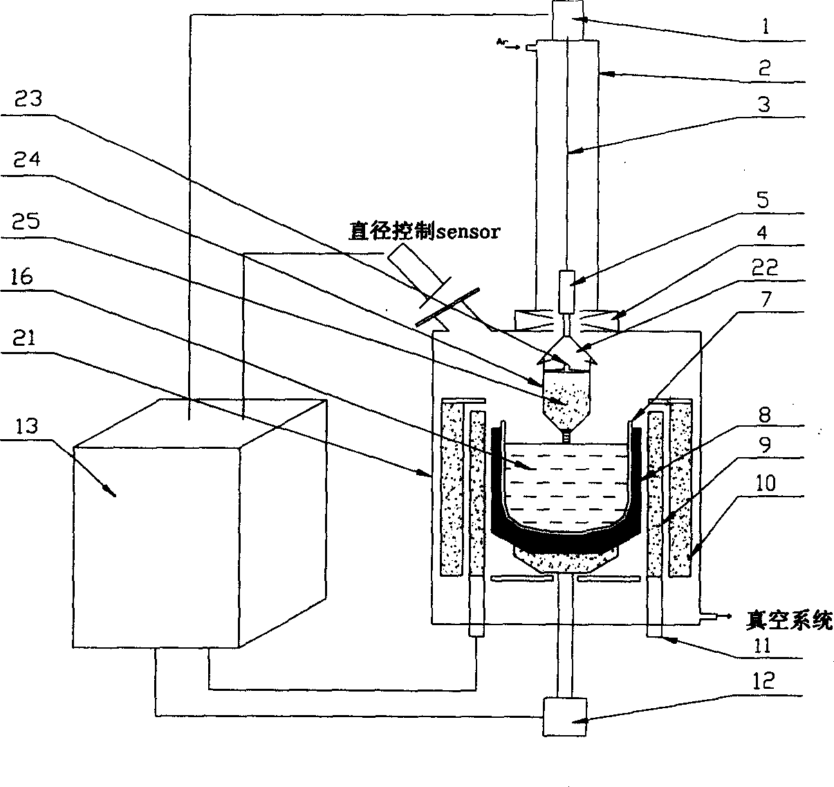
[0023] The doping funnel used for the manufacture of heavily doped Czochralski silicon single crystal has a funnel body 24, a funnel cover 23, a hook 22,

[0024] Use the doping method of doping funnel of the present invention, it is characterized in that its step is:

[0025] 1) All the polysilicon is loaded into the quartz crucible;

[0026] 2) The dopant is loaded into the doping funnel as claimed in claim 1, the funnel cover is covered, suspended under the seed chuck, and the doping funnel is raised into the auxiliary chamber, the furnace cover is covered, and the Vacuum, chemical material; after all the material is melted, lower the doping funnel to doping in the furnace of the single crystal furnace. If antimony is mixed, then lower the doping funnel to a height of 10 to 20 mm from the nozzle of the lower part of the funnel to the molten silicon surface. Let the heated and melted antimony drop into the silicon melt to be absorbed; if phosphorus or arsenic is added, lowe...


PUM


Abstract

A doping hopper for preparing the heavyly doped monosilicon by straight pulling up is composed of main body with bottom discharge spout, cover and hanging hook. Its doping method includes loading the doping agent in said hopper, fully smelting polysilicon, lowering the hopper until its discharge spout has a 10-20 mm distance from the surface of molten silicon for doping Sb, or until its discharge spout into the molten silicon by 5-10 mm depth for doping P or As, and doping. Its advantage is high doping efficiency (90-100%).

Description

technical field [0001] The invention relates to a doping method for heavy-doped Czochralski silicon single crystal production and a doping funnel thereof. Background technique [0002] Heavily doped Czochralski silicon single crystals are used to produce epitaxial substrates. Growing a high-resistivity epitaxial layer on a low-resistivity heavily doped substrate can solve the contradiction between the high breakdown voltage of bipolar transistors (requiring the use of high-resistivity silicon wafers) and low collector resistance, and can reduce bipolar transistors. The power consumption of the pole transistor is improved, and the response effect of its high-frequency signal is improved. Growing a high-resistivity silicon epitaxial layer on a low-resistivity heavily doped silicon substrate can also be used to solve the latch-up problem of CMOS components. [0003] Device manufacturing requires low substrate resistivity, but the concentration of dopa...

Claims


Application Information

Patent Timeline
Patent Type & Authority Applications(China)
IPC IPC(8): C30B15/04C30B29/06
Inventor 田达晰马向阳赵松宏杨德仁李立本
Owner 金瑞泓科技(衢州)有限公司
Learn More