Field emission element

A field emission and component technology, which is applied to electrical components, parts of discharge tubes/lamps, discharge tubes, etc., can solve the problems of uneven and uneven top of carbon nanotube arrays, and the difficulty of CVD growth process for large-area uniformity, etc. Achieve the effect of improving field emission performance and reducing non-uniformity

Inactive Publication Date: 2004-10-06
TSINGHUA UNIV +1
View PDF3 Cites 6 Cited by
  • Summary
  • Abstract
  • Description
  • Claims
  • Application Information

AI Technical Summary

Problems solved by technology

A Chinese patent application number 00121140 published on March 7, 2001, "Field Emission Display Device Utilizing Carbon Nanotubes and Its Manufacturing Method", discloses the use of carbon nanotubes as an electron emission source for field emission displays. Please refer to Figure 8 , the carbon nanotube 90 is used as the emission tip, which is sprayed into the fine hole 80 by means of ultrasonic vibration, applied voltage, etc., so this method cannot ensure the height of the carbon nanotube 90 and the flatness of the top
[0005] However, to optimize the planar field emission performance of carbon nanotube arrays, a three-level structure must be adopted. In this structure, in order to achieve the uniformity of electron emission, the carbon nanotube arrays used as cathodes need to ensure micron-level uniformity on a large area. However, it is very difficult for the CVD growth process to achieve large-area uniformity; Figure 9 The scanning micrograph of the carbon nanotube array shown shows that the top of the carbon nanotube array is extremely uneven and quite messy. In addition, the surface of the carbon nanotube array is mixed with a small amount of impurities such as catalyst particles and amorphous carbon distributed in disorder. The presence of CNTs will lead to instability and inhomogeneity in the field emission performance of carbon nanotubes, which affects the field emission performance of carbon nanotube arrays

Method used


Image

  • Field emission element
  • Field emission element
  • Field emission element

Examples


Embodiment Construction

[0018] Combine below Figure 1-7 Introduce the manufacturing method of the field emission element of the present invention

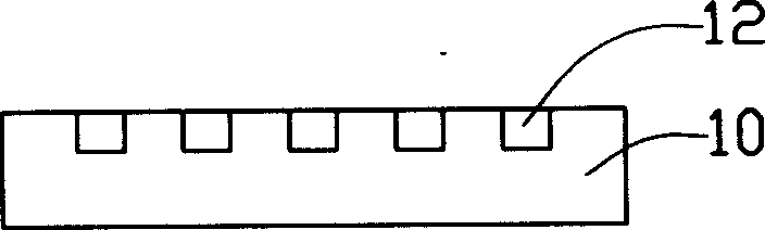
[0019] see figure 1 Firstly, a working template 10 is provided, and the working template 10 has tiny air holes 12, and the tiny air holes 12 can ensure that the working template 10 is easily desorbed in subsequent processes. The surface flatness of the working template 10 is required to be below 1 μm, and the material is required to withstand the growth temperature of carbon nanotubes at about 700° C. In this embodiment, porous silicon is selected as the working template 10 .

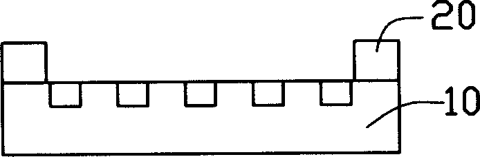
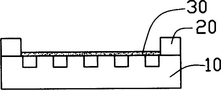
[0020] see figure 2 1. Make an insulating spacer 20 on the working template 10. In this embodiment, the mode of coating is used to make the insulating spacer 20 with a thickness of 200 μm. The method of making the insulating spacer 20 can also be printed or printed in addition to the coating method. The off-the-shelf thin plate is directly used, and the flatness of the side f...


PUM

PropertyMeasurementUnit
surface smoothnessaaaaaaaaaa

Abstract

A field emitting element is composed of a cathode, and a carbon nanotube array which is prepared by gas-phase chemical deposition method and has a growth top connected to said cathode and a growth root as the electron emitting end. Its advantages are high electron-emitting uniformity and high emitting performance.

Description

【Technical field】 [0001] The invention relates to a field emission element, especially a field emission element utilizing carbon nanotubes. 【Background technique】 [0002] Because carbon nanotubes have excellent electrical conductivity, perfect lattice structure, and nanoscale tip characteristics, they have become excellent field emission cathode materials. For details, see Walt A. de Heer et al. in Science 270, 1179-1180 (1995) , A Carbon Nanotube Field-Emission ElectronSource article, in addition, U.S. Patent No. 6,232,706 discloses a field emission element utilizing carbon nanotubes, and the field emission element disclosed in this patent includes a substrate, a catalyst deposited on the substrate, and from One or more bundles of carbon nanotube arrays grown on the catalyst are parallel to each other and perpendicular to the substrate. [0003] The field emission characteristics of carbon nanotubes have broad application prospects in fields such as field emission flat di...

Claims


Application Information

Patent Timeline
Patent Type & Authority Applications(China)
IPC IPC(8): H01J1/304H01J9/02
CPCH01J2201/30469H01J1/3044B82Y10/00H01J9/025
Inventor 刘亮范守善
Owner TSINGHUA UNIV
Why Eureka
Try Eureka