Cleaning method for mfg. appts. of semiconductor device
A technology for manufacturing equipment and semiconductors, applied in semiconductor/solid-state device manufacturing, cleaning methods and appliances, chemical instruments and methods, etc., can solve the problem that the cleaning effect of cleaning gas is not as good as that of NF3, and achieve improved cleaning effect and cleaning efficiency Effect
- Summary
- Abstract
- Description
- Claims
- Application Information
AI Technical Summary
Problems solved by technology
Method used
Image
Examples
no. 1 example
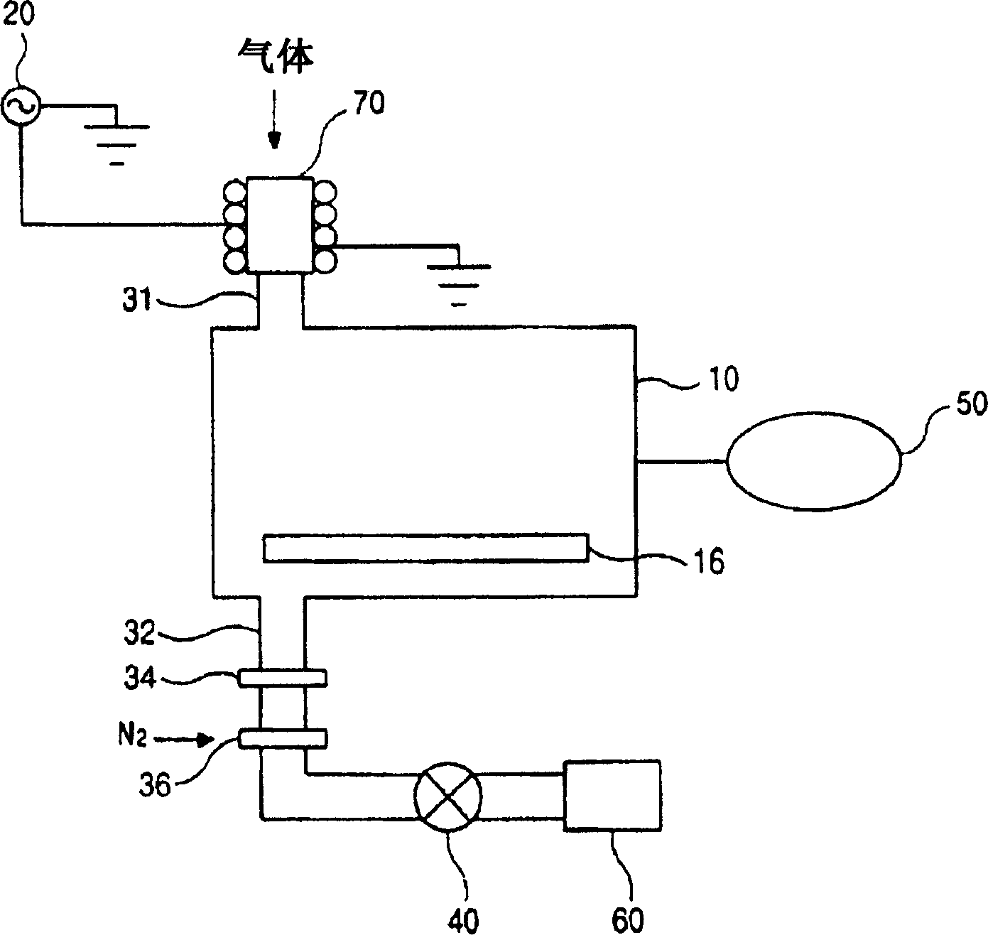
[0039] figure 1 It is a schematic diagram of equipment using the cleaning method of the manufacturing equipment of the semiconductor device according to the first embodiment of the present invention. According to the first embodiment of the present invention, the cleaning gas is activated using a remote plasma generator 70 outside the processing chamber 10 . One end of the remote plasma generator 70 is connected to a radio frequency (RF) power source 20, and the other end of the remote plasma generator 70 is grounded. A gas inlet (not shown) is connected to a remote plasma generator 70 . The plasma generated by the remote plasma generator 70 flows into the processing chamber 10 through the plasma inlet 31 . The substrate rack 16 is disposed in the processing chamber 10, and the exhaust pipe 32 is connected to the processing chamber 10 for removing residues generated during the cleaning process. The exhaust pipe 32 is also connected to the booster pump 34 and the dry pump 36...
no. 2 example
[0050] According to the second embodiment, for figure 1 The remote plasma generator 70 applies an RF source of approximately 800 watts to generate plasma, and will figure 1 The pressure of the processing chamber 10 was maintained at 400 mTorr. The other conditions of the second embodiment are exactly the same as those of the first embodiment, and the same equipment as the first embodiment is also used. In addition, samples for measuring the cleaning speed of the processing chamber were placed at three places, namely, the center of the substrate holder 16 , the side wall of the processing chamber 10 , and the front wall of the processing chamber 10 .
[0051] C 4 f 8 O is the fluorocarbon gas contained in the first cleaning gas, and N 2 O or NO is the second cleaning gas. Set the flow rate to about 40sccm C 4 f 8 O with a flow rate of about 180 sccm of O 2 into the remote plasma generator 70. No second purge gas but only C 4 f 8 O / O 2 The cleaning speed is about 118...
no. 3 example
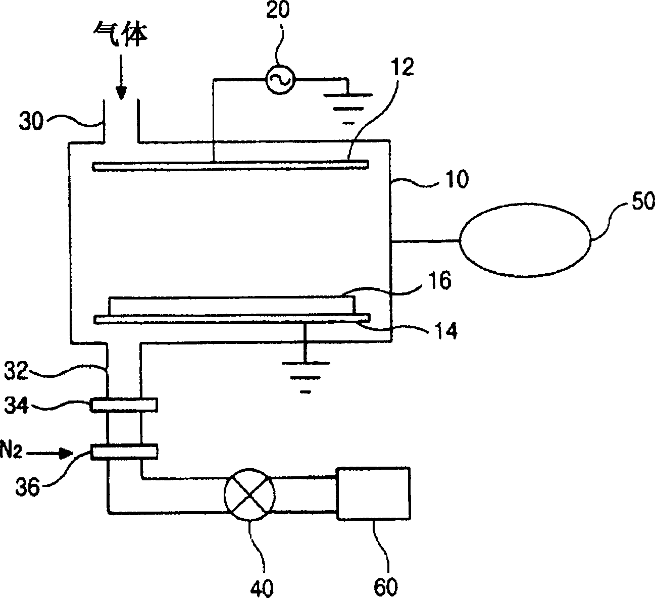
[0056] According to a third embodiment, the RF source for generating the plasma is 300 watts and the chamber pressure is 400 mTorr. A third embodiment is a capacitively coupled plasma (CCP) system.
[0057] Silicon nitride (5 cm x 5 cm) was formed on a silicon chip as a sample for measuring the cleaning speed of the process chamber. C 4 f 8 O is the fluorocarbon gas contained in the first cleaning gas, and N 2 is the second cleaning gas. Set the flow rate to 16sccm C 4 f 8 O with a flow rate of 64 sccm O 2 supplied to the processing chamber. The cleaning speed when the second cleaning gas is not used is about 507.7 nm / min, and the DRE and MMTCE are 98.38% and 3.58×10 -9 .
[0058] Introduce N as the second cleaning gas with a flow ratio of 0.05 to 0.20 to the first cleaning gas 2 , wherein the total flow rate of the first cleaning gas is 80 sccm, and the cleaning speed, DRE and MMTCE values at various flow ratios are measured.
[0059] Will N 2 added to C 4 f 8...
PUM
 Abstract
Description
Claims
Application Information
 - R&D Engineer
- R&D Manager
- IP Professional
- Industry Leading Data Capabilities
- Powerful AI technology
- Patent DNA Extraction
Browse by: Latest US Patents, China's latest patents, Technical Efficacy Thesaurus, Application Domain, Technology Topic, Popular Technical Reports.
© 2024 PatSnap. All rights reserved.Legal|Privacy policy|Modern Slavery Act Transparency Statement|Sitemap|About US| Contact US: help@patsnap.com


