Biological analogue material with surface nano array and its preparing method
A nano-array and bio-simulation technology, applied in the field of bio-simulation materials and their preparation, can solve the problems of lack of long-term stability, complicated operation, and inability to provide a large enough surface.
- Summary
- Abstract
- Description
- Claims
- Application Information
AI Technical Summary
Problems solved by technology
Method used
Image
Examples
preparation example Construction
[0045] Preparation of substrate
[0046] For the surface biomimetic material of the present invention, the substrate can use inorganic solid materials, such as semiconductor silicon, germanium, gold-plated substrates and optoelectronic devices, etc. or polymer materials, and the substrate needs to be suitable for bonding with the self-assembled layer, which can have a flat or curved surface surface.
[0047] Such as figure 1 As shown, in one embodiment of the present invention, a metal layer, such as gold, platinum, titanium, cadmium, etc., is deposited on a silicon wafer to facilitate connection with the self-assembled layer. A substrate according to another embodiment of the present invention includes a layer of titanium or cadmium with a thickness of 3-10 nanometers, and a layer of gold with a thickness of 20-500 nanometers.
[0048] In an embodiment of the invention, the metal has two layers, including a titanium layer and a gold layer. The two layers of metal can be...
Embodiment 1
[0072] Example 1 Preparation of Surface Nanoarray Material
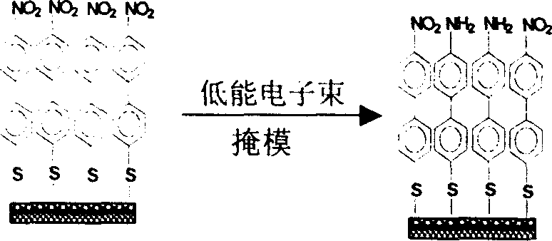
[0073] Under high vacuum conditions, 5 nanometers of titanium and 50 nanometers of gold are first deposited on a clean silicon wafer (high-purity single crystal silicon). At 105°C, immerse the gold-coated silicon wafer in concentrated H 2 SO 4 with H 2 o 2 Washed in the mixed solution and dried with nitrogen gas. Then it was immersed in 1.5 millimoles per liter of NBT ethanol solution. After the reaction was completed, it was rinsed with organic solvents such as ethanol and chloroform successively, and dried with nitrogen. Let the low-energy electron beam (300eV) generated by the Leica LION LV 1 electron beam generation system pass through the "mask" (copper grid of 40×40μm square grid array, the square grid contains round holes with a diameter of 2.3μm), and the nitro group is selected The organically modified surface nano-array material is obtained through the reduction to the amino group, that is, a solid s...
Embodiment 2
[0074] Example 2 Preparation of Surface Nanoarray Material
[0075]Under high vacuum conditions, 8 nanometers of titanium and 100 nanometers of gold were first deposited on a clean silicon wafer. At 105°C, immerse the gold-coated silicon wafer in concentrated H 2 SO 4 with H 2 o 2 Washed in the mixed solution and dried with nitrogen gas. Then immerse it in 0.01-10 millimoles per liter of NBT ethanol solution, after the reaction, rinse with organic solvents such as ethanol and chloroform successively, and blow dry with nitrogen. Let the low-energy electron beam (300eV) generated by the Leica LION LV 1 electron beam generation system pass through the "mask" (a copper grid with a square grid array of 40×40 μm, and the square grid contains round holes with a diameter of 2.3 μm), and the nitro group is selected Reduction to amino groups (J.Vac.Sci.Technol.B 19, 2732-2735, 2001), to obtain organically modified surface nanoarray materials, that is, solid support membranes with...
PUM
| Property | Measurement | Unit |
|---|---|---|
| strength | aaaaa | aaaaa |
| thickness | aaaaa | aaaaa |
| thickness | aaaaa | aaaaa |
Abstract
Description
Claims
Application Information
 - R&D
- Intellectual Property
- Life Sciences
- Materials
- Tech Scout
- Unparalleled Data Quality
- Higher Quality Content
- 60% Fewer Hallucinations
Browse by: Latest US Patents, China's latest patents, Technical Efficacy Thesaurus, Application Domain, Technology Topic, Popular Technical Reports.
© 2025 PatSnap. All rights reserved.Legal|Privacy policy|Modern Slavery Act Transparency Statement|Sitemap|About US| Contact US: help@patsnap.com


