Position design of alignment marks

A technology for aligning marks and designing structures, which is applied in the direction of photomechanical equipment, pattern surface photolithography, optics, etc. It can solve the problems affecting the correct reflection path of light and affecting the stability, so as to achieve good flatness and improve stability sexual effect

Inactive Publication Date: 2004-06-16
UNITED MICROELECTRONICS CORP
View PDF0 Cites 0 Cited by
  • Summary
  • Abstract
  • Description
  • Claims
  • Application Information

AI Technical Summary

Problems solved by technology

However, the monolithic metal platform has the problem of dishing during the chemical mechanical polishing process. The metal platform that produces the dishing phenomenon will form a depression in the middle part, which will affect the correct reflection path of the light. while also affecting the alignment stability

Method used


Image

  • Position design of alignment marks
  • Position design of alignment marks
  • Position design of alignment marks

Examples


Embodiment Construction

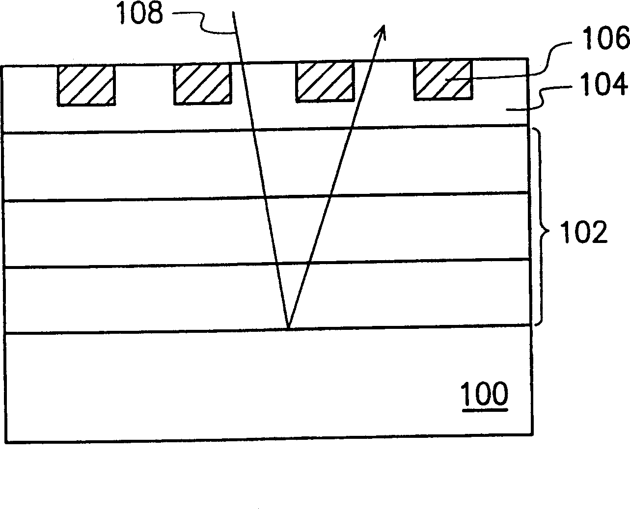
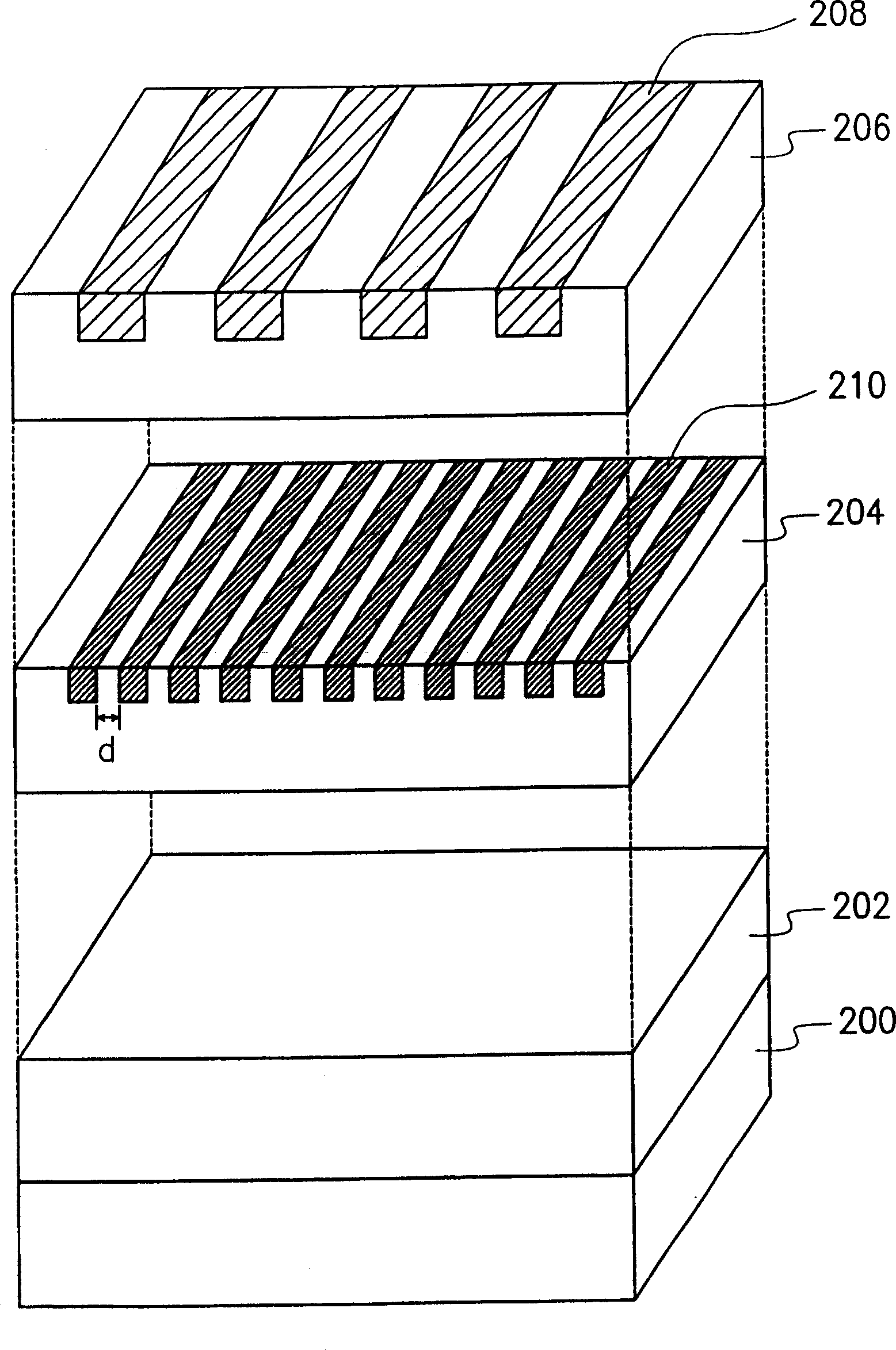
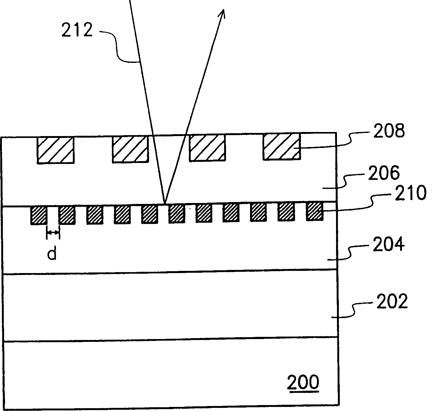
[0024] Please also refer to figure 2 as well as image 3 , figure 2 What is shown is an exploded schematic diagram of the three-dimensional structure of the position design of the non-zero layer alignment mark of the preferred embodiment of the present invention, and image 3 What is shown is a cross-sectional schematic diagram of the positional design of the non-zero layer alignment mark of the preferred embodiment of the present invention.

[0025] Depend on figure 2 and image 3 It can be seen that the alignment mark 208 is disposed in a planarized dielectric layer 206 on the semiconductor substrate 200, and the method for forming the alignment mark 208 is, for example, firstly forming several long lengths with similar positions in the dielectric layer 206. strip-shaped openings (not shown), and metal material is filled in the strip-shaped openings to form non-zero layer alignment marks composed of a plurality of metal lines. Usually, the alignment mark manufacturin...


PUM


Abstract

A position design for alignment mark which is used on the substrate having a multilayered structure, the alignment mark is arranged on the first dielectric layer of the substrate, and a metallic pattern layer is arranged in another dielectric layer below the first dielectric layer, wherein the metallic pattern layer comprises a plurality of bar shaped metal wires, and the distance between the bar shaped metal wires is smaller than the wavelength of light for aligning.

Description

technical field [0001] The present invention relates to a position design of an alignment mark (Alignment Mark), and in particular relates to a metal pattern layer arranged under the alignment mark to reflect alignment light so that the alignment mark has optimal alignment stability Alignment mark position design. Background technique [0002] Photolithography is a key step in the success or failure of manufacturing semiconductor components, so it plays a pivotal role in the semiconductor manufacturing process. Moreover, with the miniaturization and integration of semiconductor components, the precision, difficulty, complexity and frequency of exposure and lithography manufacturing processes also increase accordingly. In the exposure and photolithography manufacturing process, improper pattern transfer can lead to rework of the photoresist layer, and even lead to the scrapping of the entire wafer. Therefore, in order to make the pattern of the photomask correct Transferrin...

Claims


Application Information

Patent Timeline
IPC IPC(8): G03F7/00H01L21/027
Inventor 刘家助林思闽
Owner UNITED MICROELECTRONICS CORP
Why Eureka
Try Eureka