Level chagning circuit
A technology for converting circuits and levels, which is applied in the direction of logic circuit connection/interface layout, electrical components, electronic switches, etc., and can solve problems such as area increase
- Summary
- Abstract
- Description
- Claims
- Application Information
AI Technical Summary
Problems solved by technology
Method used
Image

Examples
Embodiment 1
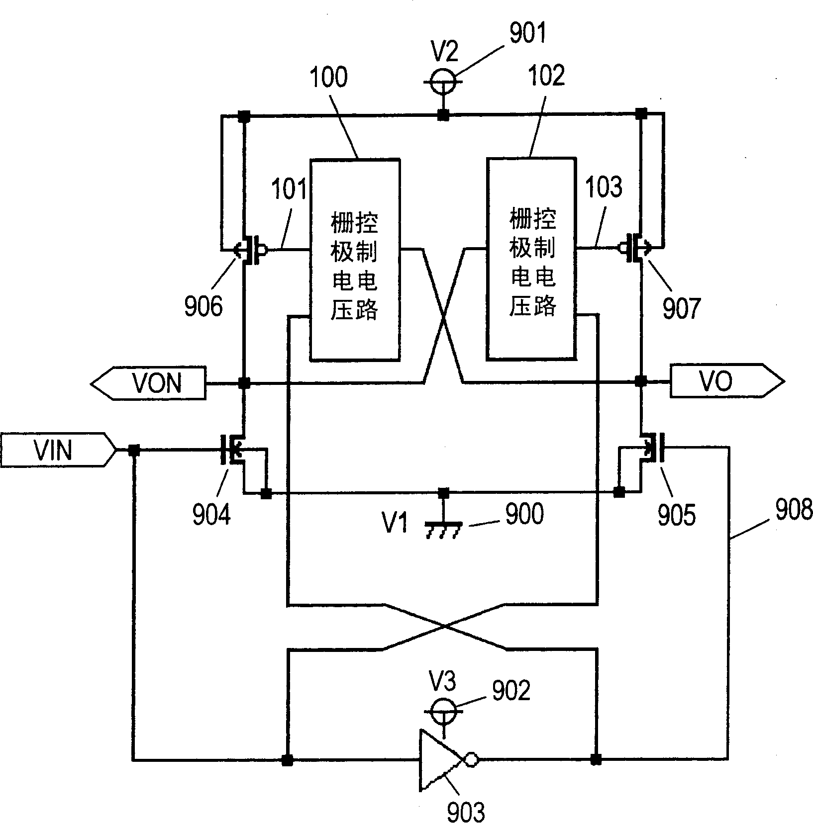
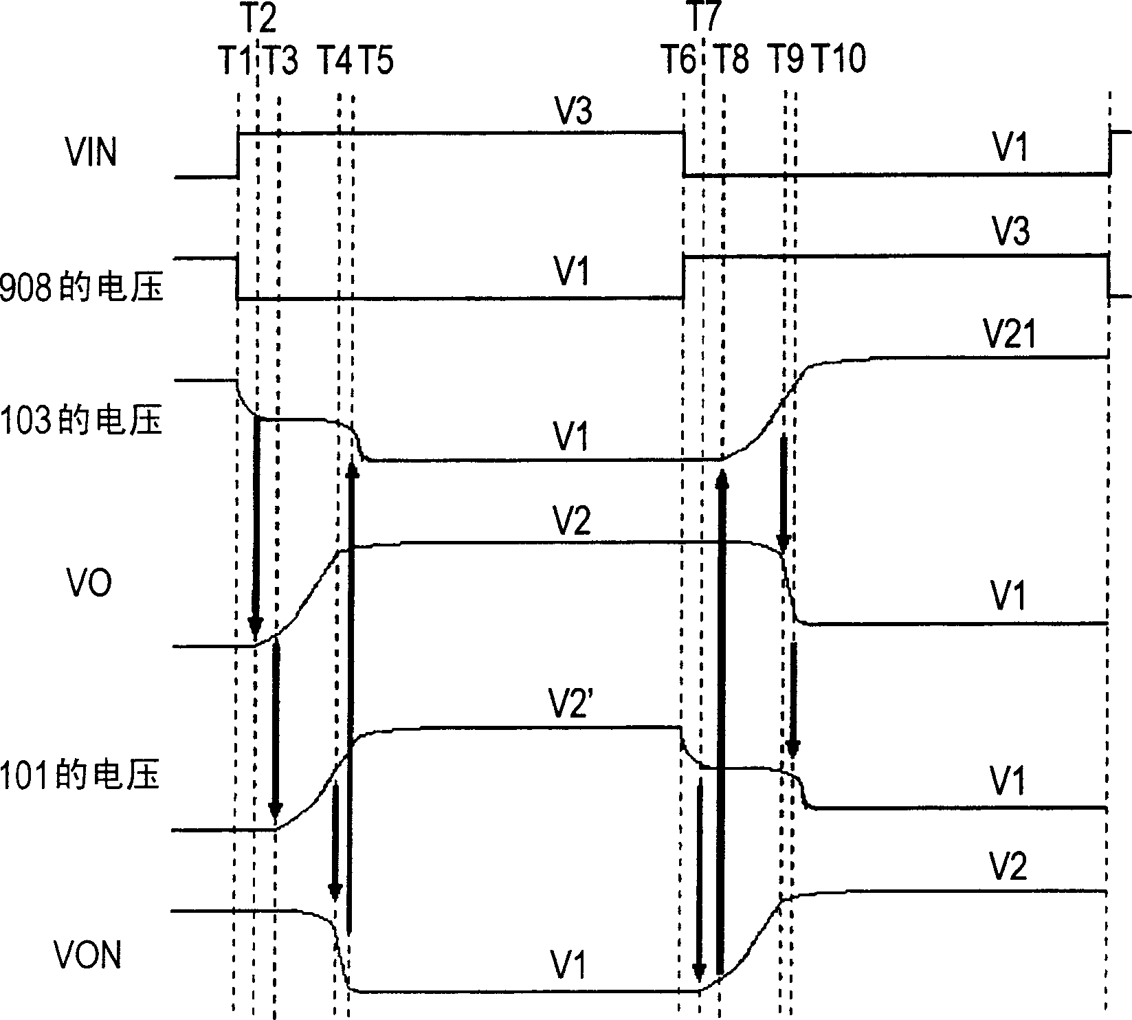
[0060] figure 1 A schematic diagram showing a level conversion circuit according to Embodiment 1 of the present invention. exist figure 1 Here, a gate voltage control circuit 100 as a first gate voltage control circuit is connected to an output terminal VO as a second terminal, and has an output terminal 101 . A gate voltage control circuit 102 as a second gate voltage control circuit is connected to an output terminal VON as a first terminal, and has an output terminal 103 . The output terminal VO is a terminal for outputting a level-shifted signal in phase with the input signal VIN as the first input signal, and the output terminal VON is a terminal for outputting a level-shifted signal of the second input signal. The second input signal is inverted from the input signal VIN.
[0061] The voltage of the power supply 900 is the voltage level V1 as the first power supply voltage, the voltage of the power supply 901 is the voltage level V2 as the second power supply voltag...
Embodiment 2
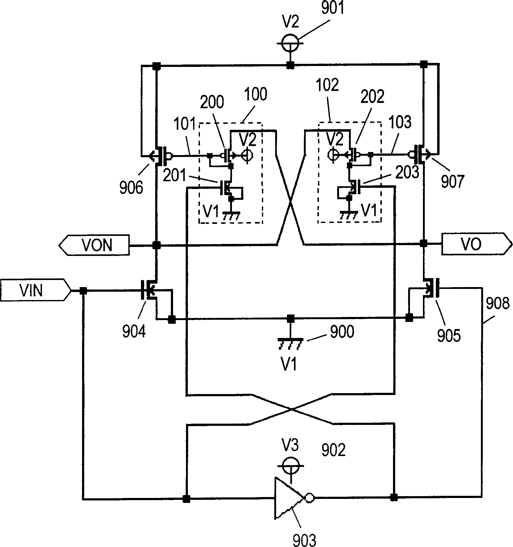
[0075] Figure 3A Shown is a level conversion circuit diagram related to Embodiment 2 of the present invention. exist Figure 3A Among them, the gate voltage control circuit 100 is connected to the output terminal VO and has an output terminal 101 . The gate voltage control circuit 102 is connected to the output terminal VON and has an output terminal 103 . In the transistor 200 , the source is connected to the output terminal VO, and the gate and drain are connected in common to the output terminal 101 . The transistor 201 receives an inverted signal 908 of the input signal VIN to its gate, and its drain is connected to the drain of the transistor 200 . In the transistor 202 , its source is connected to the output terminal VON, and its gate and drain are commonly connected to the output terminal 103 . The gate of the transistor 203 receives the input signal VIN, and its drain is connected to the drain of the transistor 202 . The second conductivity type transistor 300 (h...
Embodiment 3
[0088] Figure 4A Shown is a level conversion circuit diagram related to Embodiment 3 of the present invention.
[0089] exist Figure 4A Among them, the gate voltage control circuit 100 is connected to the output terminal VO and has an output terminal 101 . The gate voltage control circuit 102 is connected to the output terminal VON and has an output terminal 103 . The second conductivity type depletion transistor 400 (hereinafter referred to as the transistor 400) of the eleventh transistor has its source connected to the output terminal VO, and its gate and drain connected in common, so that the voltage between the gate and the source is 0V. drain current flows. The transistor 201 receives an inverted signal of the input signal VIN to its gate, and its drain is connected to the drain of the transistor 400 . The second conduction type depletion-type transistor 401 (hereinafter referred to as transistor 401) of the twelfth transistor has its source connected to the output...
PUM
 Abstract
Description
Claims
Application Information
 - R&D
- Intellectual Property
- Life Sciences
- Materials
- Tech Scout
- Unparalleled Data Quality
- Higher Quality Content
- 60% Fewer Hallucinations
Browse by: Latest US Patents, China's latest patents, Technical Efficacy Thesaurus, Application Domain, Technology Topic, Popular Technical Reports.
© 2025 PatSnap. All rights reserved.Legal|Privacy policy|Modern Slavery Act Transparency Statement|Sitemap|About US| Contact US: help@patsnap.com