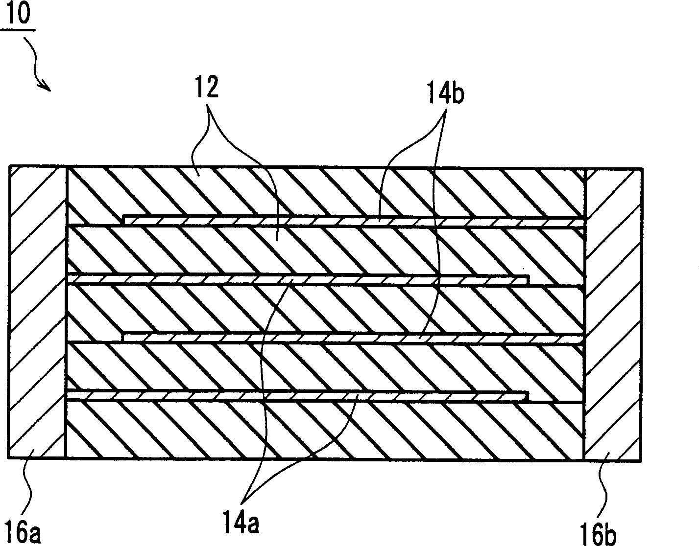
Ceramic laminated body and its manufacturing method
A manufacturing method and a technology for a laminated body, which can be applied to ceramic layered products, laminated capacitors, chemical instruments and methods, etc., and can solve problems such as metal film breakage.
- Summary
- Abstract
- Description
- Claims
- Application Information
AI Technical Summary
Problems solved by technology
Method used
Image

Examples
Embodiment 1
[0054] A ceramic laminate is produced through the following steps (1) to (6).
[0055] (1) Corresponding to the internal electrode pattern, a metal thin film is formed by a vacuum process on the support film subjected to mold release treatment (metal thin film forming step).
[0056] (2) Forming a ceramic green board on a carrier film (ceramic green board formation process).
[0057] (3) On the ceramic green sheet obtained in the above (2), an adhesive is applied corresponding to the internal electrode pattern (adhesive application process).
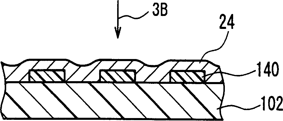
[0058] (4) The thin metal film formed on the support film obtained in (1) above is pressed onto the ceramic green sheet obtained in (3) above. In this way, only the portion of the metal thin film corresponding to the internal electrode pattern is transferred onto the ceramic green board (metal thin film transfer process).
[0059] (5) The ceramic green sheet on which the metal thin film was transferred obtained in the above (4) is pres...
Embodiment 1-b
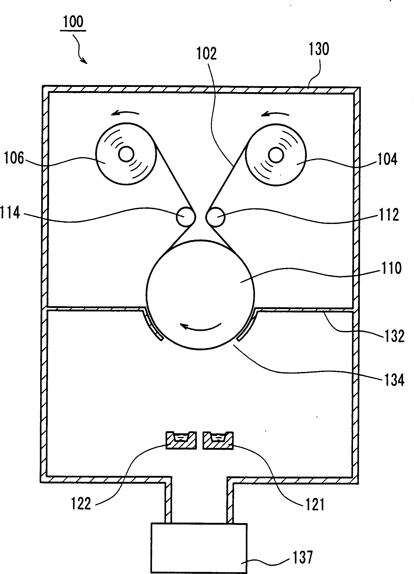
[0075] ●Example 1-b (alloy sputtering with Ni-Ba alloy as target)
[0076] An RF magnetron sputtering facility (13.56 MHz, 2 KW) in which the first thin film formation source 121 uses a Ni-Ba alloy as a target was used. The second thin film forming source 122 was not used. The barrel roll 110 was cooled so that the temperature of the support film 102 reached 10°C. The transport speed of the support film 102 was 3 nm / sec. In this manner, a metal thin film containing Ni and Ba and having a thickness of 0.6 μm was formed on the support film 102 .
[0077] Ni-Ba alloys with Ba composition ratios of 0, 1, 5, 10, 30, and 49 atm% were used as targets, and the composition ratios of Ni and Ba in the metal thin film were changed. The composition ratio was confirmed by ICP emission spectroscopic analysis. In either case, a metal thin film having a composition ratio substantially the same as that of the target was obtained.
[0078] As the support film 102, a PET sheet subjected to t...
Embodiment 1-c
[0079] ●Example 1-c (2-source sputtering with Ni and Ti as targets)
[0080]A DC sputtering facility in which the first thin film formation source 121 uses Ti as a target was used. Furthermore, a DC sputtering facility in which the second thin film formation source 122 uses Ni as a target was used. The barrel roll 110 was cooled so that the temperature of the support film 102 reached 10°C. In this way, a metal thin film containing Ni and Ti with a thickness of 0.8 μm was formed on the support film 102 .
[0081] Along the moving direction of the support film 102, a Ti sputtering device 121 is arranged on the upstream side, and a Ni sputtering device 122 is arranged on the downstream side, so that the metal thin film composed of Ni and Ti formed on the support film 102 , the closer to the support film 102 side, the larger the Ti content, and the closer to the opposite side, the larger the Ni content. Auger electron spectroscopic analysis was performed on the obtained metal t...
PUM
| Property | Measurement | Unit |
|---|---|---|
| thickness | aaaaa | aaaaa |
| thickness | aaaaa | aaaaa |
Abstract
Description
Claims
Application Information
 - R&D
- Intellectual Property
- Life Sciences
- Materials
- Tech Scout
- Unparalleled Data Quality
- Higher Quality Content
- 60% Fewer Hallucinations
Browse by: Latest US Patents, China's latest patents, Technical Efficacy Thesaurus, Application Domain, Technology Topic, Popular Technical Reports.
© 2025 PatSnap. All rights reserved.Legal|Privacy policy|Modern Slavery Act Transparency Statement|Sitemap|About US| Contact US: help@patsnap.com