Nonvolatile memory for catching charges in isolative films
A non-volatile memory technology, applied in the structure of data readout and high-speed readout of data, can solve the problems of activation of the delay amplifier circuit, inability to generate readout data at high speed, and inability to achieve high-speed access, etc. Achieve high-speed and accurate readout
- Summary
- Abstract
- Description
- Claims
- Application Information
AI Technical Summary
Problems solved by technology
Method used
Image
Examples
Embodiment 2
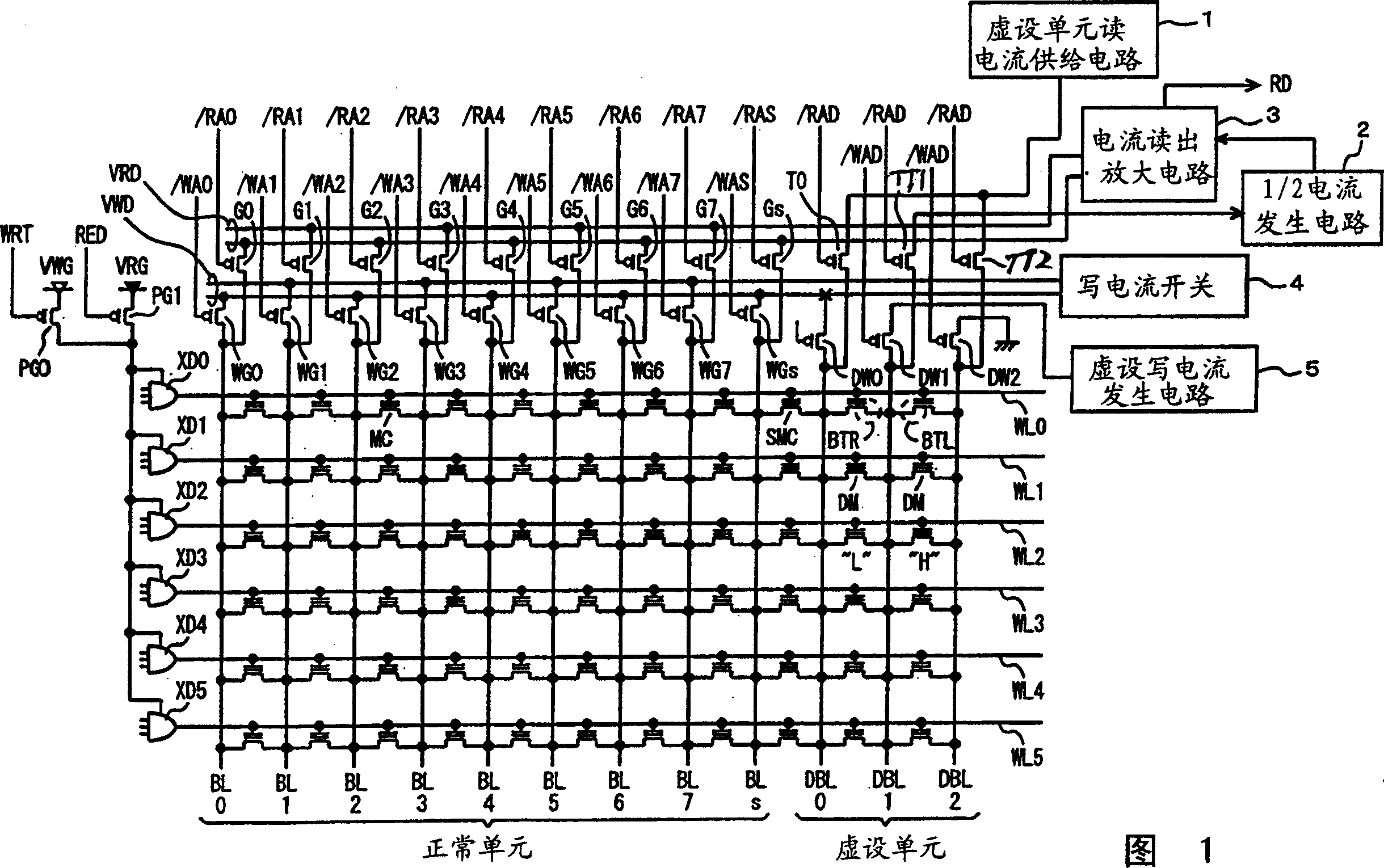
[0148] FIG. 5 is a diagram schematically showing the configuration of important parts of a nonvolatile semiconductor memory according to Embodiment 2 of the present invention. The structure shown in FIG. 5 differs from the structure shown in FIG. 1 in the following points. That is, when data is read, a dummy read current i is supplied to dummy bit lines DBL0 and DBL2 , and a reference current generating circuit 30 that generates the average current and transmits it to the current amplifier circuit 3 is provided. In addition, dummy bit line DBL1 is connected to the ground node through this read selection gate TT1 when data is read. The other structures are the same as those shown in FIG. 1, and the corresponding parts are denoted by the same reference numerals, and detailed description thereof will be omitted.
[0149] In the configuration shown in FIG. 5, dummy bit line DBL1 is connected to the ground node when data is read. The reference current generating circuit 30 suppli...
Embodiment 3
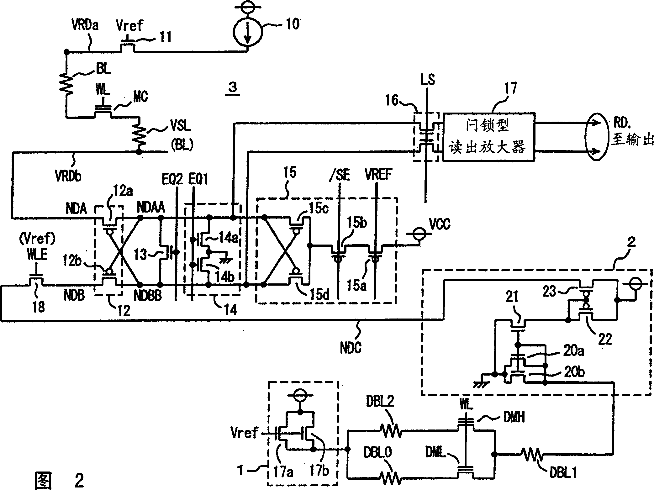
[0159] Figure 7 It is a structural diagram showing important parts of the nonvolatile semiconductor memory according to Embodiment 3 of the present invention. exist Figure 7 In this example, the current sense / amplifier circuit 3 has the same structure as that of the first and second embodiments. However, this current read / amplifier circuit 3 compares the current flowing through the internal read data line VRDa with the current supplied from the subtraction circuit 45 , unlike the first and second embodiments described above. That is, in the Figure 7 In the configuration shown, the current sense / amplifier circuit 3 uses the current obtained by subtracting the current flowing through the memory cell from the reference current as a comparison object.
[0160] In this third embodiment, dummy cells DM and normal cells MC are arranged in a straight line within the same array. The structure of the memory cell array in Embodiment 3 is the same as that of the memory cell array s...
Embodiment 4
[0183] FIG. 9 is a structural diagram showing important parts of a nonvolatile semiconductor memory according to Embodiment 4 of the present invention. In Embodiment 4, dummy cells and normal cells are also arranged in rows and columns in the same array. Even in the configuration of Example 4 shown in FIG. 9 , the residual current was used as a comparison object.
[0184] In order to generate a reference current for comparison with the residual current of the memory cell current, an average current (Ih+I1) is provided that supplies the read current to the dummy cells DMH and DML and generates the currents Ih and I1 flowing in these dummy cells DMH and DML. ) / 2 residual current and the current supply circuit 55 that generates a mirror current of the current from the current generation circuit 50 and supplies the mirror current to the current read / amplifier circuit 3.
[0185] The current generating circuit 50 supplies a read current to these dummy cells DMH and DML, and discha...
PUM
 Abstract
Description
Claims
Application Information
 - R&D
- Intellectual Property
- Life Sciences
- Materials
- Tech Scout
- Unparalleled Data Quality
- Higher Quality Content
- 60% Fewer Hallucinations
Browse by: Latest US Patents, China's latest patents, Technical Efficacy Thesaurus, Application Domain, Technology Topic, Popular Technical Reports.
© 2025 PatSnap. All rights reserved.Legal|Privacy policy|Modern Slavery Act Transparency Statement|Sitemap|About US| Contact US: help@patsnap.com


