Capacitor, semiconductor device and its manufacture method, electrooptical device and electronic machine
A manufacturing method, semiconductor technology, applied in the direction of semiconductor/solid-state device manufacturing, semiconductor devices, fixed capacitor dielectrics, etc., can solve the problems of not being able to use glass, deprivation of freedom, and not being able to form aluminum wiring, etc., to achieve high withstand voltage and uniformity sex high effect
- Summary
- Abstract
- Description
- Claims
- Application Information
AI Technical Summary
Problems solved by technology
Method used
Image

Examples
Embodiment 1
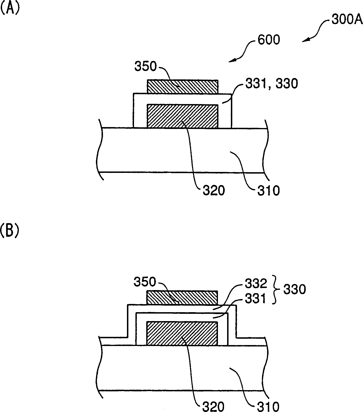
[0072] figure 1 (A) and (B) are cross-sectional views schematically showing the structures of the semiconductor devices of Embodiment 1 and its modification of the present invention, respectively.
[0073] exist figure 1 In (A), in the semiconductor device 300A of this embodiment, a capacitor 600 having a lower electrode 320 made of a tantalum film as a dielectric and other semiconductor elements (not shown) are formed on a substrate 310. An insulating layer 330 of the first layer and an upper electrode 350 made of a silicon film or a metal film doped with impurities.
[0074] Here, the entire lower electrode 320 is made of a tantalum film, and the insulating layer 330 is made of a tantalum oxide film 331 obtained by oxidizing the surface of the tantalum film.
[0075] When manufacturing the semiconductor device 300A having such a structure, in the present embodiment, after the tantalum film (metal film for insulating layer formation) is formed on the substrate 310, the surf...
Embodiment 2
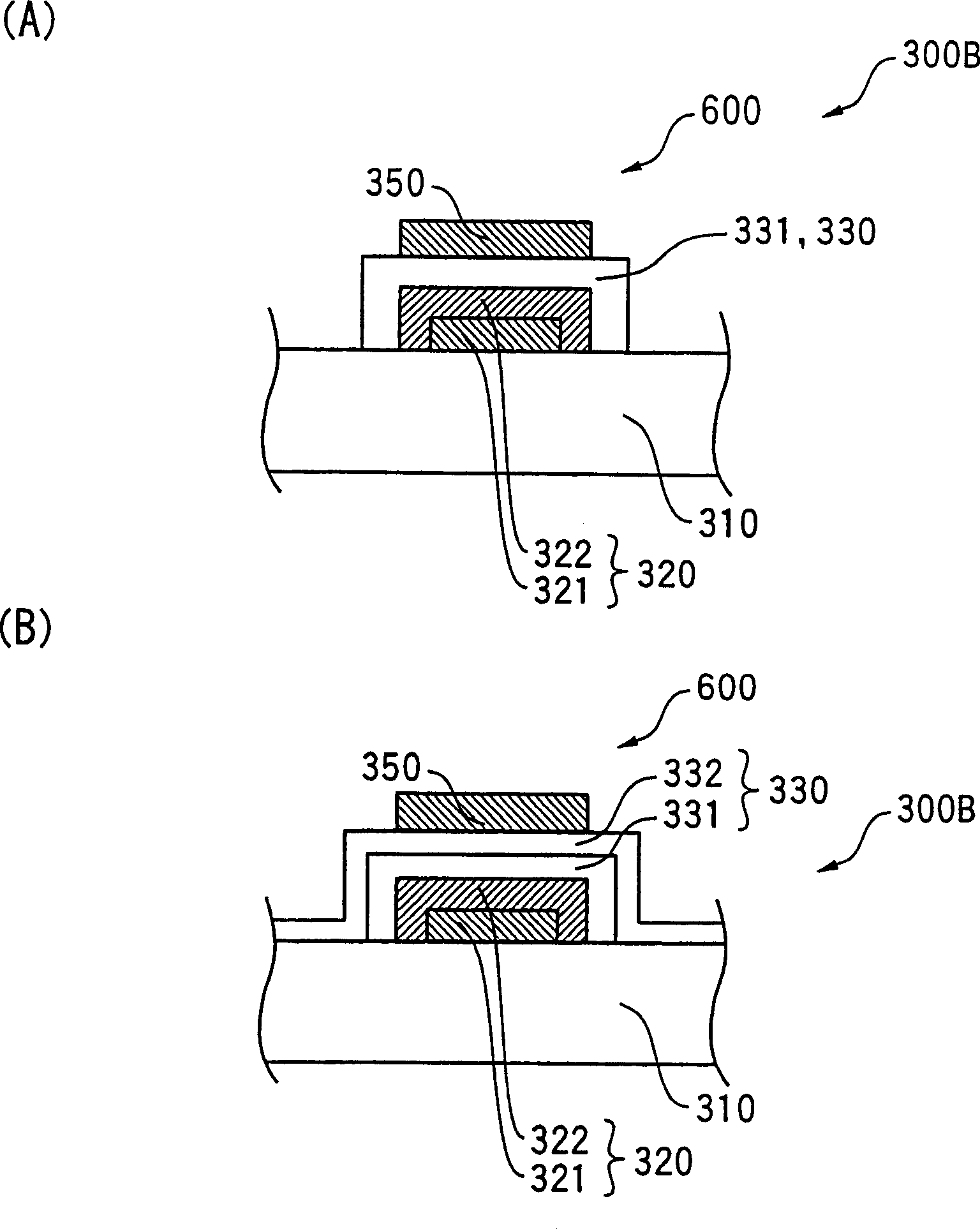
[0080] figure 2 (A) and (B) are cross-sectional views schematically showing the structures of semiconductor devices according to Embodiment 2 and its modification of the present invention, respectively.
[0081] exist figure 2 In (A), in the semiconductor device 300B of the present embodiment, a capacitor 600 having a lower electrode 320, an insulating layer 330 as a dielectric layer, and other semiconductor elements (not shown) are formed on a substrate 310. and an upper electrode 350 made of a silicon film or a metal film doped with impurities.
[0082] Here, the lower electrode 320 is composed of a lower electrode layer 321 and an upper electrode layer 322, the lower electrode layer 321 is composed of a metal film such as an aluminum film, a chromium film, or a silicon film doped with impurities, and the upper electrode layer 322 is composed of The upper layer side of the lower layer side electrode layer 321 is composed of a tantalum film layered thereon.
[0083] When...
Embodiment 3
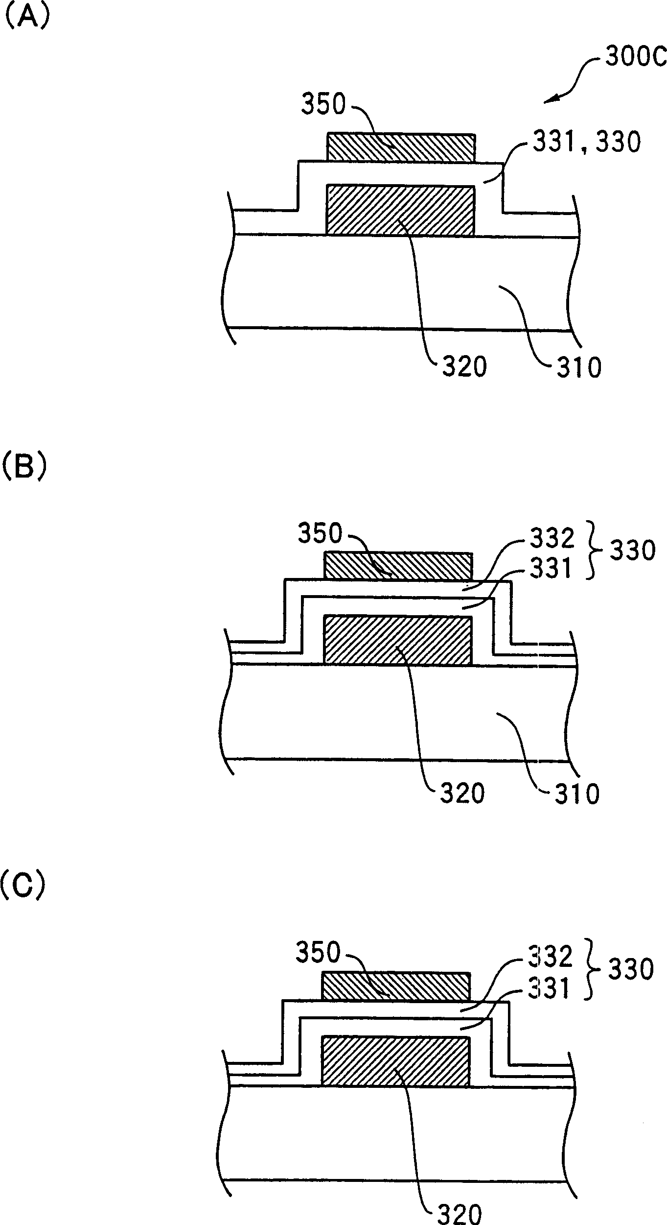
[0088] image 3 (A) and (B) are cross-sectional views schematically showing the structures of semiconductor devices according to Embodiment 3 and its modifications of the present invention, respectively.
[0089] exist image 3 In (A), in the semiconductor 300C of the present embodiment, a capacitor 600 having a lower electrode 320, an insulating layer 330 as a dielectric layer, and other semiconductor elements (not shown) are formed on a substrate 310. The upper electrode 350 is formed of a silicon film or a metal film doped with impurities.
[0090] Here, the lower electrode 320 is a silicon film or a metal film doped with impurities, and the insulating layer 330 is composed of a tantalum oxide film 331 obtained by oxidizing a tantalum film.
[0091] When manufacturing the semiconductor device 300C having such a structure, in this embodiment, after the lower electrode 320 is formed on the substrate 310, a tantalum film (metal film for forming an insulating layer) is formed...
PUM
 Abstract
Description
Claims
Application Information
 - R&D
- Intellectual Property
- Life Sciences
- Materials
- Tech Scout
- Unparalleled Data Quality
- Higher Quality Content
- 60% Fewer Hallucinations
Browse by: Latest US Patents, China's latest patents, Technical Efficacy Thesaurus, Application Domain, Technology Topic, Popular Technical Reports.
© 2025 PatSnap. All rights reserved.Legal|Privacy policy|Modern Slavery Act Transparency Statement|Sitemap|About US| Contact US: help@patsnap.com