Switch power source
A technology of switching power supply and switching circuit, which is applied in 66 fields, can solve problems such as deterioration of stability, prolonged time interval, and increased loss of rectification circuit, so as to reduce losses, prevent the generation of direct current, and prevent the effects of direct current
- Summary
- Abstract
- Description
- Claims
- Application Information
AI Technical Summary
Problems solved by technology
Method used
Image
Examples
Embodiment approach 1
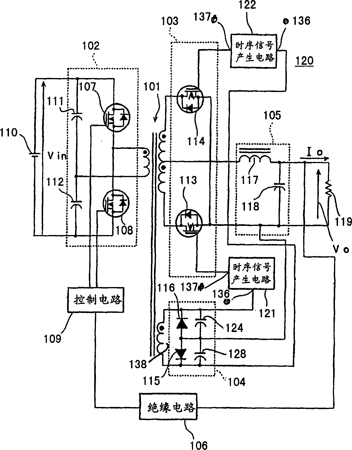
[0081] figure 1 is a circuit diagram of the switching power supply 120 in the first embodiment of the present invention.
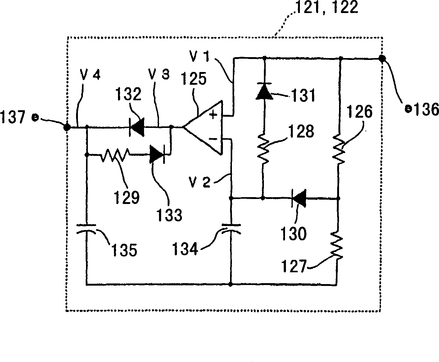
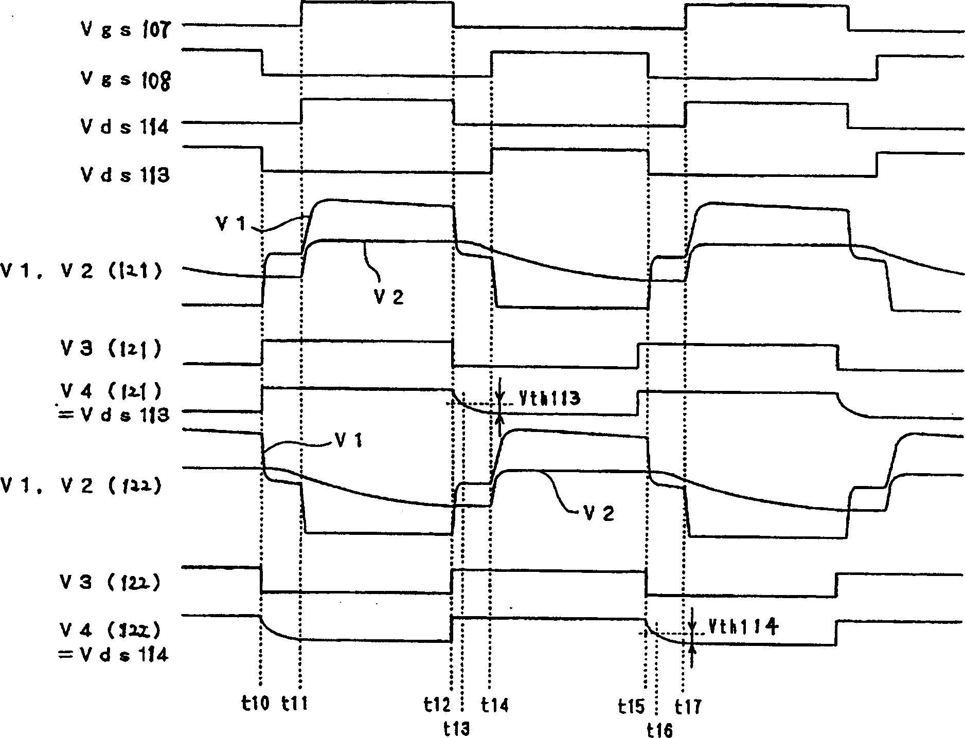
[0082] Such as figure 1 As shown, the switching power supply 120 of the first embodiment of the present invention is a synchronously rectified power supply of a typical conventional switching power supply of the so-called half-bridge type. However, the difference of the switching power supply 120 of this embodiment of the present invention is that the first timing signal generating circuit 121 is inserted between the rectifying transistor driving circuit 104 and the gate of the first rectifying transistor 113, and the rectifying transistor driving A second timing signal generating circuit 122 is inserted between the gate of the circuit 104 and the second rectifying transistor 114; its difference is that the first auxiliary capacitor 123 is connected to both ends of the first diode 115, and the The two ends of the second diode 116 are connected to the s...
Embodiment approach 2
[0111] A second embodiment of the present invention will be described in detail below with reference to the accompanying drawings, wherein like components are denoted by like characters and their descriptions are omitted. This embodiment of the present invention is specific for carrying out the present invention, and the present invention is not limited to this embodiment described here.
[0112] Figure 8 It is a circuit diagram of a switching power supply; Figure 9 is when the sum of the dead time and the transformer leakage commutation time is equal to the switching delay time of the synchronous rectification element, Figure 8 A timing diagram of each partial voltage / current waveform in the switching power supply shown; Figure 10 It is the timing diagram of each part of the voltage / current waveform when the transformer leakage commutation time is shorter than the switching delay period of the switching power supply synchronous rectification element in the switching pow...
Embodiment approach 3
[0156] A third embodiment of the present invention will be described below with reference to the drawings.
[0157] Figure 13 is a circuit diagram of the switching power supply 330 in the third embodiment of the present invention.
[0158] Such as Figure 13 As shown, the switching power supply 330 in this embodiment of the present invention employs a primary circuit comprising a bark converter circuit and a half bridge circuit, which are connected in series as conventional switching power supplies. The difference between the switching power supply 330 and the traditional (third related technology) switching power supply is that the rectifying circuit 55 in the traditional switching power supply is replaced by the rectifying circuit 331, and the control circuits 332 and 333 replace the control circuit 63 in the traditional switching power supply . As for the rest, since the switching power supply in the present invention is structurally similar to a conventional switching ...
PUM
 Abstract
Description
Claims
Application Information
 - R&D
- Intellectual Property
- Life Sciences
- Materials
- Tech Scout
- Unparalleled Data Quality
- Higher Quality Content
- 60% Fewer Hallucinations
Browse by: Latest US Patents, China's latest patents, Technical Efficacy Thesaurus, Application Domain, Technology Topic, Popular Technical Reports.
© 2025 PatSnap. All rights reserved.Legal|Privacy policy|Modern Slavery Act Transparency Statement|Sitemap|About US| Contact US: help@patsnap.com


