
Double insulation layer thin film field emitting cathode

A field emission cathode and insulating layer technology, used in electrical components, parts of discharge tubes/lamps, circuits, etc., can solve the problem of less than 0.1%, has not been well developed and applied, and cannot meet large-screen high-brightness display devices, etc., to achieve the effect of long life and high withstand voltage

Inactive Publication Date: 2002-06-05
TSINGHUA UNIV +1
View PDF0 Cites 6 Cited by
  • Summary
  • Abstract
  • Description
  • Claims
  • Application Information

AI Technical Summary

Problems solved by technology

Since the affinity of silicon material reaches 4 electron volts, the electron emission rate is generally less than 0.1%, which cannot meet the needs of large-screen high-brightness display devices.
After this MISM structure was proposed, due to the unsolved problems above, this structure has not been well developed and applied, and has basically been abandoned.

Method used


Image

  • Double insulation layer thin film field emitting cathode
  • Double insulation layer thin film field emitting cathode
  • Double insulation layer thin film field emitting cathode

Examples


Embodiment 1

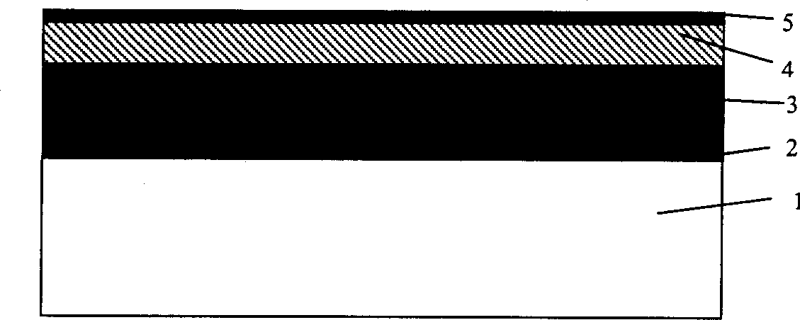
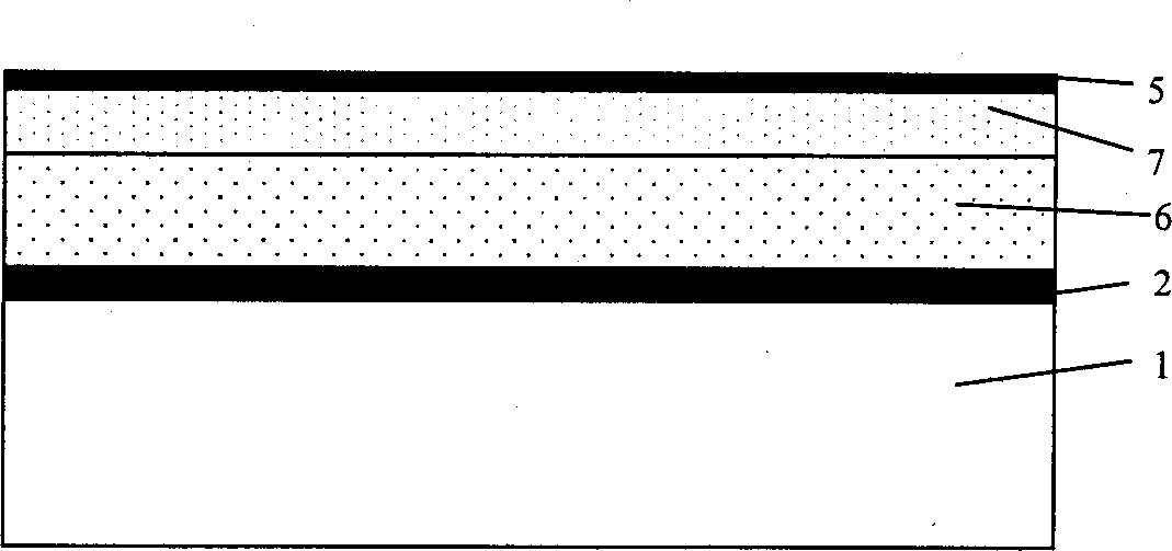
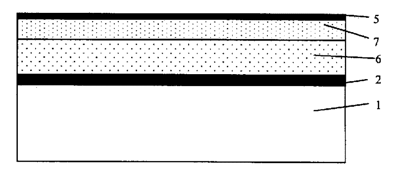
[0019] The lower electrode layer adopts a metal-semiconductor structure, and the lower metal film and the upper semiconductor film are respectively 100 nanometers thick metal molybdenum and 30 nanometers thick zirconium nitride film. The lower insulating layer and the upper insulating layer are respectively 200 nanometer silicon dioxide and 50 nanometer calcium oxide films. The upper electrode layer adopts a single-layer gold film with a thickness of 7 nanometers. At a driving voltage of 60 V, field emission with an emissivity exceeding 0.5% was obtained.

Embodiment 2

[0021] The lower electrode layer adopts a 100 nanometer single-layer semiconductor zirconium nitride film. The lower insulating layer and the upper insulating layer are respectively 200 nanometer silicon dioxide and 50 nanometer calcium oxide films. The upper electrode layer adopts a single-layer gold film with a thickness of 7 nanometers. At a driving voltage of 60 V, field emission with an emissivity exceeding 0.5% was obtained.

Embodiment 3

[0023] The lower electrode layer adopts a metal-metal structure, and the lower metal film and the upper metal film are respectively 100 nanometers thick molybdenum and 50 nanometers thick dysprosium film. The lower insulating layer and the upper insulating layer are respectively 200 nanometer silicon dioxide and 50 nanometer calcium oxide films. The upper electrode layer uses a 10 nm thick gold film. At a driving voltage of 80 V, field emission with an emissivity exceeding 0.5% was obtained.


PUM


Abstract

A film field emission cathode with double insulated layers belongs to the technique area of vacuum electron emission type of flat display device. The invention incldues glass base plate, lower electrode layer, insulating layer and upper electrode layer. The insulating layer is composed of upper nad lower insulating films, usually the lower insulating layer is non-crystal insulating film and the upper insulating layer is crystal insulating film. The lower electrode layer can be composed of two layers of metal films or can be composed of a metal and semi-conductor film. The upper electrode layer can be composed of two layers of metal films or a metal and conductor film. The invention gives electron emissivity large than 0.5%. The non-crystal insulating film has property of high withstandingvoltage and long service life.

Description

Technical field: [0001] The invention belongs to the technical field of vacuum electron emission flat panel display, and in particular relates to a novel planar double insulating layer film field emission cathode. Background technique: [0002] Field emission cathodes include structures such as microtip type (Spindt type), diamond film type, carbon nanotube type, metal-insulator-metal type (MIM) and metal-insulator-semiconductor layer-metal type (MISM), among which The present invention is relatively close to the DC MISM structure. The MISM structure consists of a glass substrate, a lower electrode layer, an insulating layer, a semiconductor layer and an upper electrode layer. [0003] Among the various MISM structures currently used, the glass substrate is usually flat glass with an ion isolation layer, and the ion isolation layer can be thin films such as silicon dioxide, aluminum oxide, and silicon nitride; the lower electrode layer is made of aluminum, gold, Molybdenum...

Claims


Application Information

Patent Timeline
Patent Type & Authority Applications(China)
IPC IPC(8): H01J1/304
Inventor 李德杰万媛卜东生王红光
Owner TSINGHUA UNIV
Learn More