
Optical device and spectroscope and polarization separating device using the device

An optical device and beam technology, applied in the field of optical devices and beam splitter devices, can solve the problems of large device size and inability to realize polarization separation, etc.

Inactive Publication Date: 2002-04-03
NIPPON SHEET GLASS CO LTD
View PDF0 Cites 10 Cited by
  • Summary
  • Abstract
  • Description
  • Claims
  • Application Information

AI Technical Summary

Problems solved by technology

Therefore, in order to improve the performance of an optical demultiplexer employing a diffraction grating, the problem of large device size inevitably arises
[0012] In addition, angle-dependent polarization separation cannot be achieved with general diffraction gratings since there is no difference in diffraction angle in the polarization direction

Method used


Image

  • Optical device and spectroscope and polarization separating device using the device
  • Optical device and spectroscope and polarization separating device using the device
  • Optical device and spectroscope and polarization separating device using the device

Examples


example 1

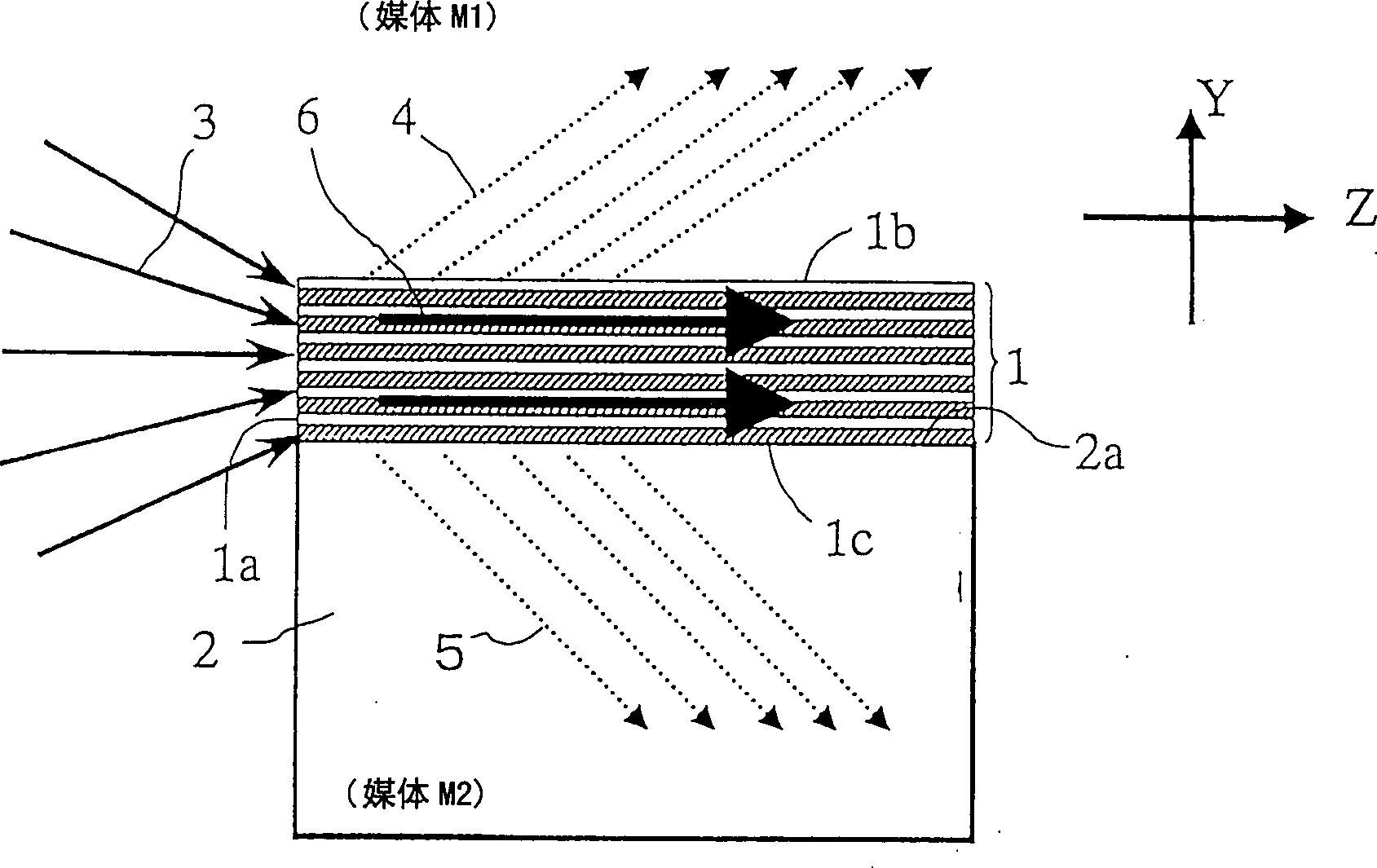
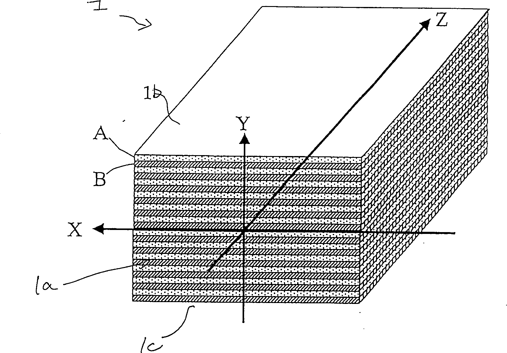
[0136] Such as Figure 15 As shown, a multilayer film 1 is formed on the surface of a parallel plane substrate 2 (soda lime carbonate glass) having a thickness of 1 mm. The thickness of the substrate 2 can generally be selected within the range of 0.1 to 2 mm. Silicon dioxide film (thickness t 1 =150nm) and titanium oxide film (thickness t 2 = 150nm) are successively formed on the substrate surface to form a period. After repeating this operation for a total of 20 cycles (40 layers), a silicon dioxide film with a thickness of 2 μm was attached thereto as protective film 7 .

[0137] Two opposite end faces 2c of the substrate were cut perpendicular to the other surfaces of the substrate and polished to a width of 10 mm. The optical system shown in FIG. 16 was used so that the laser beam was incident on the end face 1a of the multilayer film portion (6 µm thickness).

[0138] A wavelength-tunable laser is used as laser source 11 . After the laser beam 20 is emitted from th...

example 2

[0141] A multilayer film 1 is formed on the surface of a parallel plane substrate 2 (quartz glass) having a thickness of 1 mm. Titanium oxide film (thickness t 1 =212nm) and silicon dioxide film (thickness t 2 = 212nm) are successively formed on the substrate surface to form a period. This operation is repeated for a total of 20 cycles (40 layers). The surface of the multilayer film 1 tangential to the air is a silicon dioxide layer.


PUM

PropertyMeasurementUnit
Thicknessaaaaaaaaaa
Thicknessaaaaaaaaaa
Thicknessaaaaaaaaaa

Abstract

An optical device in which an end surface of a periodic multilayer structure is provided as a beam incidence surface or as a beam exit surface. The optical device can realize a high resolving-power spectroscopic apparatus without having any increase in size of the apparatus and by use of good directivity of beam leaked from the multilayer structure and strong wavelength dependence of an angle of the leaked beam.

Description

technical field [0001] The present invention relates to optical devices and spectroscopic arrangements for use in optical communication systems, optical measurement systems or the like. Background technique [0002] In particular, the present invention relates to a novel technique suitable for splitting a beam into beam components with different wavelengths in an optical device of a beam splitter, or splitting a beam into optical components with different polarization directions in a polarization splitting optical device. [0003] Due to the rapid promotion of the optical fiber communication network on the Internet, there is a strong demand for increasing the capacity of the optical fiber communication network. Wavelength Division Multiplexing (WDM) communications have made rapid progress as a means of increasing capacity. Optical functional devices with good wavelength selectivity, such as optical demultiplexers, filters or splitters, are required for this kind of WDM comm...

Claims


Application Information

Patent Timeline
IPC IPC(8): G01J3/12G01J3/447G02B5/28G02B6/10G02B6/122G02B6/34G02B27/28
CPCG02B6/34G02B6/10G01J3/447G02B5/285G02B27/283G01J3/12B82Y20/00G01J3/0256G02B6/1225
Inventor 橘高重雄奈良正俊中泽达洋小山正浅井贵弘
Owner NIPPON SHEET GLASS CO LTD
Learn More