Method for constructing well structures for hybrid optical waveguide and the optical waveguide

A technology of optical waveguide and optical core, applied in the direction of optical waveguide light guide, light guide, optics, etc., can solve the problem of reduction of optical signal transmission

Inactive Publication Date: 2007-01-24
INTEL CORP
View PDF5 Cites 0 Cited by
  • Summary
  • Abstract
  • Description
  • Claims
  • Application Information

AI Technical Summary

Problems solved by technology

If the wells are not formed properly, voids may form in the wells where they cannot be

Method used


Image

  • Method for constructing well structures for hybrid optical waveguide and the optical waveguide
  • Method for constructing well structures for hybrid optical waveguide and the optical waveguide
  • Method for constructing well structures for hybrid optical waveguide and the optical waveguide

Examples


Embodiment Construction

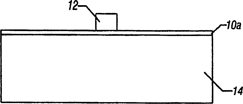
[0036] Reference attached figure 1 In the cross-sectional view of , the substrate 14 may be covered by the lower cladding layer 10 . The lower cladding layer can be a material such as silicon. The optical core 12 may form ridges or lines on the lower cladding 10 . Such as figure 1 As shown, the axis of the ridge is positioned perpendicular to the transverse plane. The optical core can be, for example, a silicon doped with germanium or an oxynitride material.

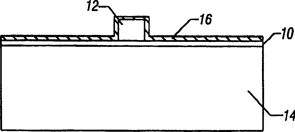
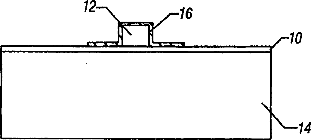
[0037] Such as figure 2 As shown, a thin seed layer 16 of metallic material such as nickel is formed across the optical core 12 and lower cladding layer 10 . In one embodiment, the metal 16 may be deposited. A first mask is formed on the seed layer 16 using standard photolithography processes. Then the seed layer 16 is etched into the required pattern, as attached image 3 Shown in cross section. Wet etching is very advantageous for this etching process because the seed layer 16 can be completely removed from t...


PUM


Abstract

A well may be formed for access to an optical waveguide core by a process that results in an L-shaped well. The L-shaped well may then be filled with a polymer. By controlling the size of each portion of well, the occurrence of bubbles within the well and cuts to the core may be reduced.

Description

technical field [0001] The present invention generally relates to well-shaped hole structures for hybrid optical waveguides. Background technique [0002] An optical waveguide is a structure that transmits optical signals. In general, an optical waveguide may include an optical core surrounded by upper cladding and lower cladding. Most optical signals are typically transmitted in the optical core along the axis of the waveguide structure. [0003] In order to access the optical core, a well-shaped hole may be formed through the upper cladding. This well-shaped hole is formed by etching the upper cladding. Sometimes, such etching does not fully expose the optical core of the waveguide, resulting in reduced access to the optical signal. In other cases, the waveguide core is not only exposed but may also be damaged by the etching process, resulting in reduced optical signal transmission. [0004] After the well-shaped hole is formed, polymer can be filled into the well-sha...

Claims


Application Information

Patent Timeline
IPC IPC(8): G02B6/10H01L21/00G02B6/12G02B6/122
CPCG02B2006/12176G02B6/1221G02B6/136G02B2006/12097G02B2006/12169
Inventor U·特兰D·A·G·迪肯S·M·李
Owner INTEL CORP
Why Eureka
Try Eureka