Semiconductor memory and voltage application method to semiconductor memory

A storage element and semiconductor technology, which is applied in the fields of semiconductor devices, semiconductor/solid-state device manufacturing, static memory, etc., can solve the problems of few rewriting times, unfavorable large-capacity, large storage unit size, etc., to prevent rewriting. The effect of reducing the number of times, improving reliability, and preventing the reduction of the number of rewrites

Inactive Publication Date: 2005-12-28
PANASONIC CORP
View PDF0 Cites 0 Cited by
  • Summary
  • Abstract
  • Description
  • Claims
  • Application Information

AI Technical Summary

Problems solved by technology

For example, flash memory, because the size of the storage unit is small, it is conducive to large capacity, but the number of rewriting is not much
On the other hand, ferroelectric memory can be rewritten many times, but it is not conducive to large-capacity due to the large size of the memory cell.

Method used


Image

  • Semiconductor memory and voltage application method to semiconductor memory
  • Semiconductor memory and voltage application method to semiconductor memory
  • Semiconductor memory and voltage application method to semiconductor memory

Examples


Embodiment Construction

[0062] Hereinafter, an embodiment of the present invention will be described with reference to the drawings.

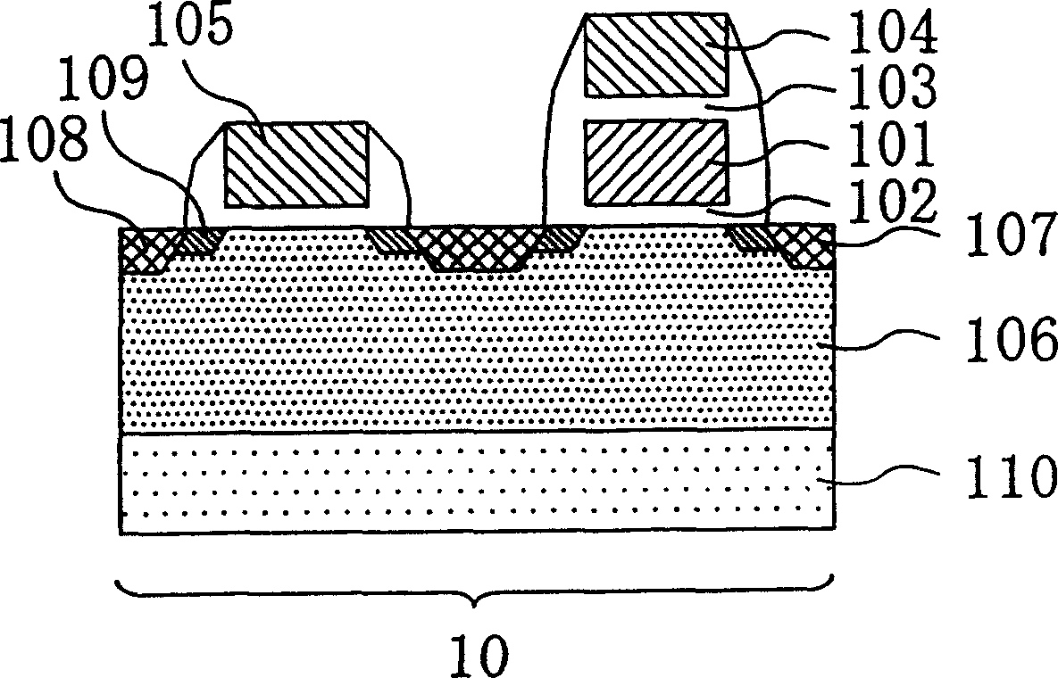
[0063] figure 1 It is an example of a semiconductor memory according to an embodiment of the present invention, and is a cross-sectional view showing part of a 1-bit memory cell (semiconductor memory element) 10 constituted by two transistors (corresponding to first and second transistors).

[0064] figure 1 The memory cell 10 shown has: a floating gate 101, a tunnel oxide film 102, an interlayer film 103 such as ONO, a control gate 104 connected to a control word line, a gate 105 connected to a selection word line, a P well 106, A source 107 connected to a source line, a drain 108 connected to a data line, a thin N-type diffusion layer 109 , and an N well 110 .

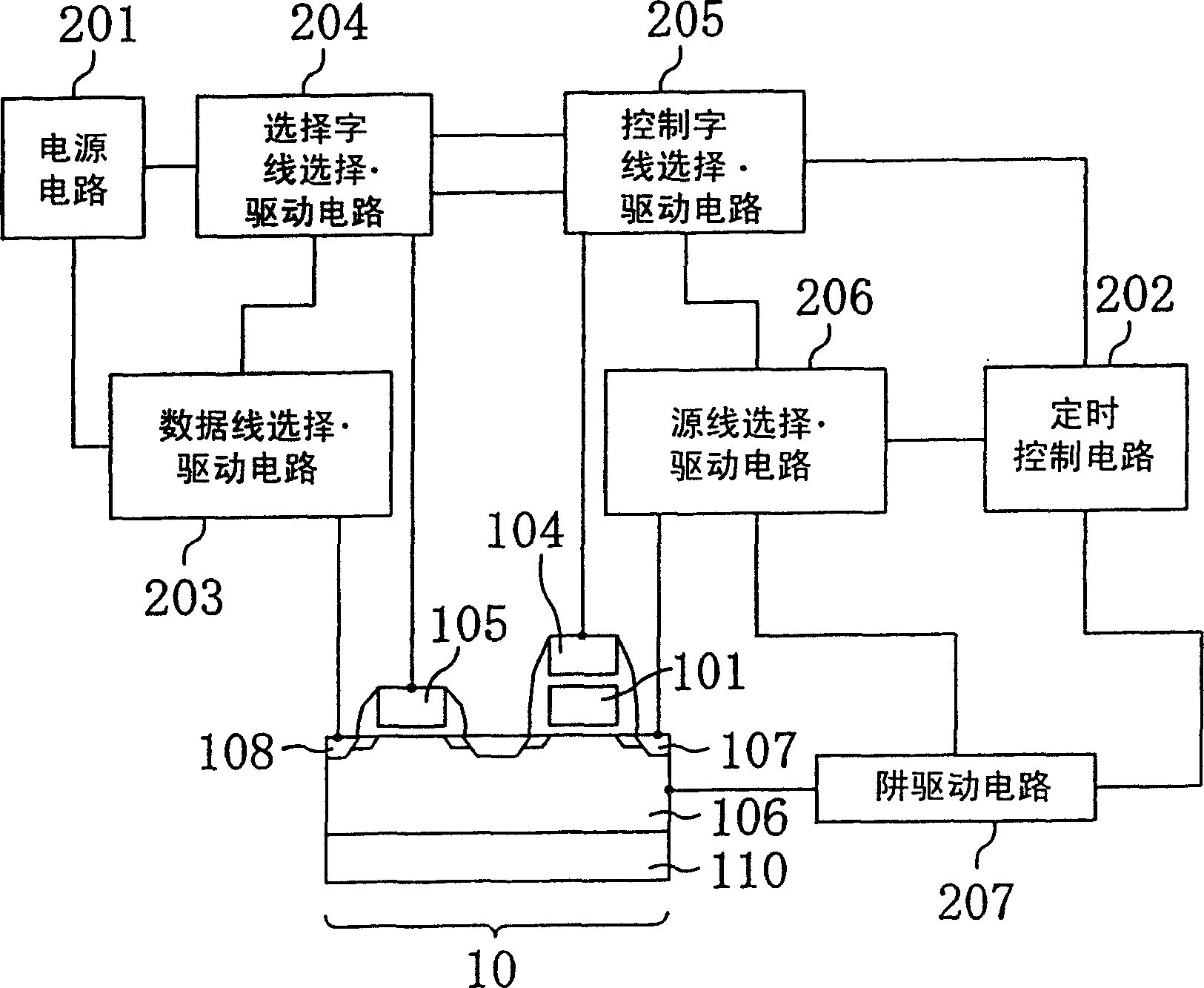
[0065] figure 2 is to show figure 1 The shown configuration example of a circuit in which the memory cell 10 operates.

[0066] figure 2 The circuit shown has: a power supply circuit 201 for gener...


PUM


Abstract

The present invention provides a semiconductor memory and a method of applying a voltage to a semiconductor memory element capable of preventing a peak electric field from being applied to a tunnel oxide film, thereby preventing a reduction in the number of times of rewriting or a reduction in data retention characteristics. The semiconductor memory of the present invention has: a storage unit (10) and a control word line selection drive circuit (205), a well drive circuit (207) and a source line selection drive circuit (206), when the floating gate in the storage unit (10) (101) a pulse generating circuit (301), a delay circuit (302), a delay circuit (303) and a delay circuit (304) outputting a pulse signal (S1) when injecting electrons. And, the control word line selection drive circuit (205) receives the delay signal (S2) from the delay circuit (302) to change the potential of the control word line, and the well drive circuit (207) receives the delay signal (S3) from the delay circuit (303). ) changes the potential of the well, and the source line selection drive circuit (206) receives the delay signal (S4) from the delay circuit (304) to change the potential of the source line.

Description

technical field [0001] The present invention relates to a semiconductor memory and a method of applying a voltage to a semiconductor memory element. Background technique [0002] In recent years, with the popularization of portable devices and the demand for energy saving and waste reduction, there has been an increasing demand for semiconductor devices incorporating nonvolatile memories that can rewrite data and retain data even when the power is turned off. As semiconductor nonvolatile memory, there are flash memory and ferroelectric memory, each of which has advantages and disadvantages, and each has its own characteristics in the field of products used. For example, flash memory, because the size of the storage unit is small is conducive to large capacity, but the number of times of rewriting is not much. On the other hand, ferroelectric memory has many times of rewriting, but since the size of the memory cell is also large, it is not conducive to increasing the capacit...

Claims


Application Information

Patent Timeline
Patent Type & Authority Patents(China)
IPC IPC(8): G11C16/02G11C16/04G11C16/06G11C16/10G11C16/14G11C16/32H01L21/8247H01L27/115H01L29/788H01L29/792
CPCG11C16/0433G11C16/10G11C16/14G11C16/32
Inventor 茶谷茂雄松浦正则
Owner PANASONIC CORP
Why Eureka
Try Eureka