Image sensor single-layer conductor rest secondary semi-etching mfg. method

A technology of image sensor and lead frame, which is applied in semiconductor/solid-state device manufacturing, electric solid-state device, semiconductor device, etc. It can solve the problems that affect the transmission effect of micro-sensing signals, it is not easy to ensure good product quality, and the preparation process is difficult. , to avoid the mechanical stamping production process, the practical effect is ideal, and the effect of quality assurance

Inactive Publication Date: 2005-04-06
谢志鸿
View PDF0 Cites 0 Cited by
  • Summary
  • Abstract
  • Description
  • Claims
  • Application Information

AI Technical Summary

Problems solved by technology

However, this stacking method involves the dimensional accuracy of the upper and lower layers of templates 81, 82. For image sensor chip packaging with a small area and a large number of pins 84, 85, delicate pins, and high precision requirements, this preparation The process is also difficult, and it is not easy to ensure good product quality; moreover, the contact resistance of the two lead frame templates 81, 82 is also a problem, and it is not easy to control it to a uniform level, which will affect the effect of micro-sensing signal transmission. Need for improvement

Method used


Image

  • Image sensor single-layer conductor rest secondary semi-etching mfg. method
  • Image sensor single-layer conductor rest secondary semi-etching mfg. method
  • Image sensor single-layer conductor rest secondary semi-etching mfg. method

Examples


Embodiment Construction

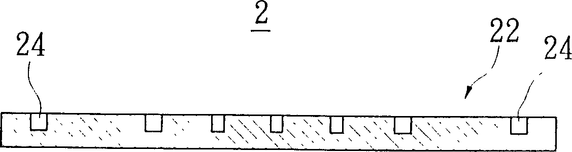
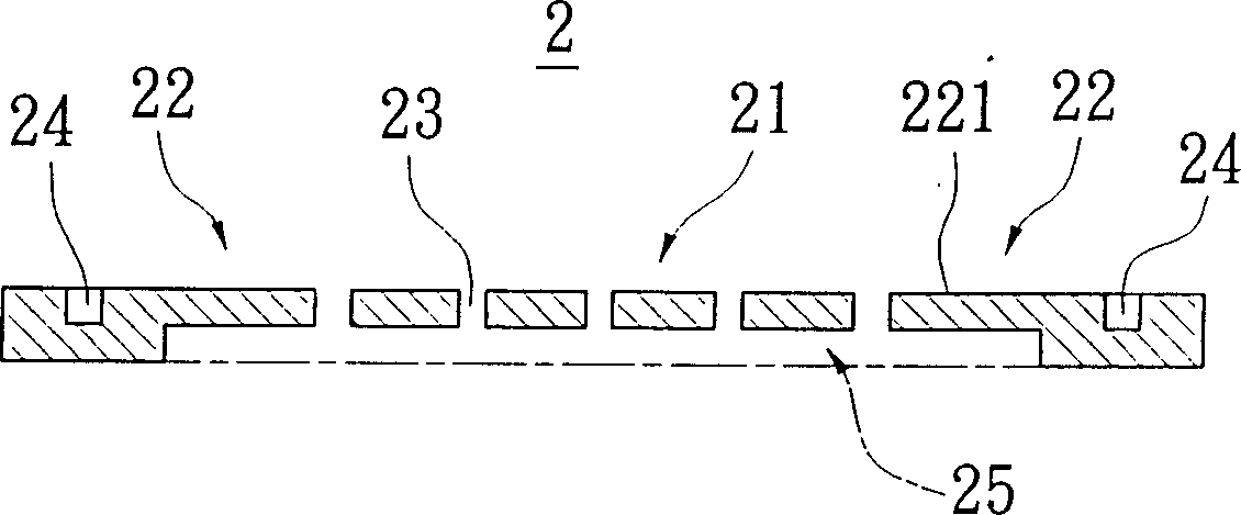
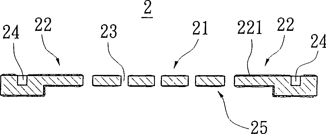
[0025] refer to Figure 1 to Figure 5 As shown, the present invention relates to a second half-etching preparation method of a single-layer lead frame of an image sensor.

[0026] Such as Figure 5 As shown, the structure of the image sensor of the present invention includes: a sensing chip 1, a single-layer lead frame 2 and a glass cover 4; the lead frame is provided with a chip holder 21 and several pins 22, and each pin 22 is surrounded inside The periphery of the chip holder 21 is defined as an inner lead 221, which is used to connect the signal contact of the sensing chip 1, and each lead 22 extends outside to the lower edge of the package to define an outer lead 222, which It is a surface mount technology pin used for soldering an external printed circuit board to transmit electrical signals; the sensing chip 1 is pasted on the top surface of the chip holder 21, and is connected to the top surface of each inner pin 221 with a metal wire 11, so that the sensing chip 1 T...


PUM


Abstract

A package of image sensor is composed of sensor chip, single-layer wiring body with chip holder and pins, glass cover plate, and plastics for sealing. Its preparing process includes semi-etching on top surface of plate substrate to form chip holder and pins, semi-etching recess structure, inlay plastics by moulding for electric isolating, electroplating the etched wiring body, inlaying it in premould, adhering sensor chip to its holder, soldering leading wires of pins, and adhering glass cover plate.

Description

technical field [0001] The invention relates to an image sensor, in particular to a method for preparing a single-layer lead frame of an image sensor with a two-time half-etching preparation method for manufacturing a three-dimensional structure of a chip seat and a pin. Background technique [0002] refer to Figure 6 to Figure 9 As shown, it is an existing image sensor (Image sensor) packaging technology, and the existing lead frame (Lead frame) manufacturing method is punching or stacking. Among them, the stamping manufacturing method is to etch the position and shape of the die pad 71 and each pin (Lead) 72 on the flat conductor substrate first, and then stamp the die pad 71 from the bottom to make it float out. Pin 72 plane. In addition, the stamping method also has the method of directly stamping the conductor plate, and directly punching out the three-dimensional structure of the chip holder 71 and each pin 72, but both of these methods need to be processed by mechan...

Claims


Application Information

Patent Timeline
Patent Type & Authority Patents(China)
IPC IPC(8): H01L21/48H01L21/56H01L21/58H01L21/60H01L21/98H01L23/48H01L27/146
CPCH01L2924/01078H01L2924/16195H01L2224/48091H01L2224/48247
Inventor 王鸿仁
Owner 谢志鸿
Why Eureka
Try Eureka