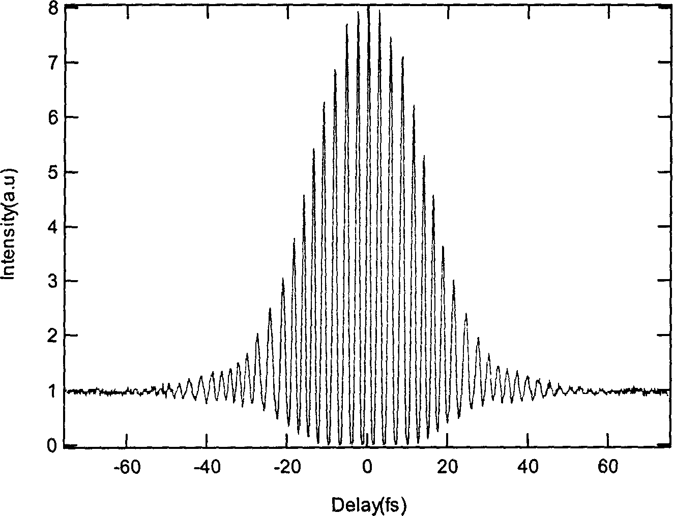
Miniaturized femto-second-solid laser oscillator
A technology of femtosecond lasers and oscillators, applied in the laser field, can solve problems such as difficulty in unifying output parameters, inability to adjust pulse width, difficulty in starting mode-locking, etc., and achieve the effect of ease of use and small and compact overall structure
- Summary
- Abstract
- Description
- Claims
- Application Information
AI Technical Summary
Problems solved by technology
Method used
Image
Examples
Embodiment 1
[0027] Such as image 3 As shown, each of the components and figure 1 Correspondingly, all are installed on the bottom plate with a size of 550×200mm. The specific parameters and installation requirements for component selection are as follows:
[0028] The focus lens 1 has a focal length of 10 cm and a diameter of 2 cm, and is placed on an adjustment frame and a translation table that can adjust the lifting and left and right positions. The laser crystal 2 is a titanium-doped sapphire crystal cut by Brewster's angle, with a size of 4×4×5 mm, and is placed on an adjustment frame and a translation stage that can adjust the pitch and angle. The first plano-concave total mirror 3 and the second plan-concave total mirror 4 have a radius of curvature of 100mm, a diameter of 12.7mm, and a thickness of 6mm. The material is crown glass and the relative distance is about 105mm. ; Among them, the concave surface of the first plano-concave total mirror 3 is plated with 532nm anti-reflection...
Embodiment 2
[0030] The specific parameters and installation of each element are as in Example 1, but the size of the climber is 20×20mm, which is plated with a 45-degree incident all-reflective dielectric film in the 700-900nm band.
Embodiment 3
[0032]The specific parameters and installation of each component are as in Example 1. However, 9 is a plane total mirror, a crown glass substrate with a diameter of 25.4mm and a thickness of 4mm is coated with a broadband dielectric film that totally reflects the wavelength of 700-900nm under normal incidence; 8 is a plane output mirror, and the aperture is 25.4 A fused silica substrate with a thickness of 2 mm and a thickness of 2 mm is coated with a dielectric film with a transmittance of 10% in the 750-850 nm band under normal incidence. There is no need to climb the mirror 12 and the gold-plated mirror 13 at this time.
PUM
| Property | Measurement | Unit |
|---|---|---|
| Focal length | aaaaa | aaaaa |
| Caliber | aaaaa | aaaaa |
| Thickness | aaaaa | aaaaa |
Abstract
Description
Claims
Application Information
 - Generate Ideas
- Intellectual Property
- Life Sciences
- Materials
- Tech Scout
- Unparalleled Data Quality
- Higher Quality Content
- 60% Fewer Hallucinations
Browse by: Latest US Patents, China's latest patents, Technical Efficacy Thesaurus, Application Domain, Technology Topic, Popular Technical Reports.
© 2025 PatSnap. All rights reserved.Legal|Privacy policy|Modern Slavery Act Transparency Statement|Sitemap|About US| Contact US: help@patsnap.com


