


Quick Research
Generate reliable direction feasibility study reports for your R&D in just a few steps.

Technical Q&A
Discover and master advanced knowledge NOW. Basics, ideas, possibilities, all at once.

Find Solutions
As an expert in R&D theories, this can generate solutions to your technical problems instantly.

Evaluate Feasibility
Analyze your overall solution with one click, know your potential R&D risks in advance.

Monitor Landscape
Get weekly tech updates, stay abreast of the latest tech innovations and key insights.
Integrated film with wave absorbing and shielding functions and preparation method thereof
A technology of integrated film and function, which is applied in the field of communication, can solve the problems of difficult processing, can not be made thin, thick film thickness, etc., and achieve the effect of overcoming processing difficulty, overcoming ultra-thin, and improving shielding bandwidth
- Summary
- Abstract
- Description
- Claims
- Application Information
AI Technical Summary
Problems solved by technology
Method used
Image

Examples
Embodiment 1
[0115] The preparation method of embodiment 1 integrated film
[0116] 1. Pretreatment of the carrier film layer
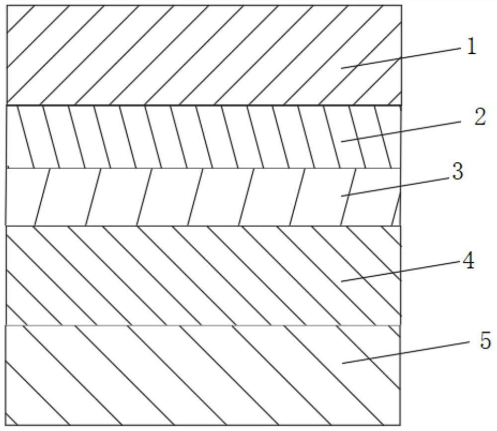
[0117] Corona pretreatment is performed on one side surface of a PET polyester film (PET) with a thickness of 25 μm and a width of 600 mm. Dyne value ≥ 32 dyne, preferably 35-60 dyne), to obtain the bearing film layer 1;
[0118] The pretreatment method of the surface of the carrier film layer can also be plasma treatment, embossing treatment, grinding, laser or UV treatment. The carrier film is pretreated to increase adhesion to the film surface. The voltage of 5000-20000V during corona treatment is suitable for the present invention.
[0119] The carrier film layer of the present invention may also be a polymer film such as PEN, PP, PI, etc. The carrier film layer with a thickness of 12-150 μm is suitable for the present invention.
[0120] 2. Preparation of absorbing material layer
[0121] 2-1. Preparation of absorbing paint:
[0122] Mix the raw materia...
Embodiment 1A
[0157] The preparation method of embodiment 1A integrated film
[0158] 1. Pretreatment of the carrier film layer
[0159] Same as Example 1.
[0160] 2. Preparation of absorbing material layer
[0161] Same as Example 1.
[0162] 3, superimposed metal layer
[0163] 3-1) Superimpose the base metal film layer
[0164] Except that the nickel target is selected for magnetron sputtering, the superimposed base metal film layer 3 is a metal nickel layer, and the thickness is 0.15 μm (usually 0.01-1 μm, preferably 0.1-0.3 μm) and step 3- 1) the same;
[0165] 3-2) Superimpose and thicken the metal film layer
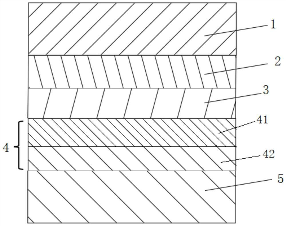
[0166] A metal nickel film with a thickness of 6 μm (usually 1-30 μm, preferably 3-6 μm) is plated on the surface of the base metal nickel film by the method of alkaline electroplating, that is, the thickened metal film 4 (such as figure 1 ); Wherein alkaline electroplating prepares the technological condition of thick metal nickel layer as follows: pH value of electrop...
Embodiment 2
[0170] The preparation method of embodiment 2 integrated film
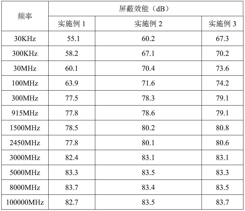
[0171] Except that the thickness of the absorbing material layer in step 2-4 is 30 μm, the rest is the same as that in Example 1.
PUM
| Property | Measurement | Unit |
|---|---|---|
| thickness | aaaaa | aaaaa |
| thickness | aaaaa | aaaaa |
| thickness | aaaaa | aaaaa |
Abstract
Description
Claims
Application Information
 - R&D Engineer
- R&D Manager
- IP Professional
- Industry Leading Data Capabilities
- Powerful AI technology
- Patent DNA Extraction
Browse by: Latest US Patents, China's latest patents, Technical Efficacy Thesaurus, Application Domain, Technology Topic, Popular Technical Reports.
© 2024 PatSnap. All rights reserved.Legal|Privacy policy|Modern Slavery Act Transparency Statement|Sitemap|About US| Contact US: help@patsnap.com