Double-chip stacked packaging structure and method
A packaging structure and packaging method technology, applied in the direction of semiconductor/solid-state device parts, semiconductor devices, electrical components, etc., can solve the problems of small product capacity, low single-chip efficiency, etc., to increase product capacity, increase production, and save stacking effect of space
- Summary
- Abstract
- Description
- Claims
- Application Information
AI Technical Summary
Problems solved by technology
Method used
Image
Examples
Embodiment approach
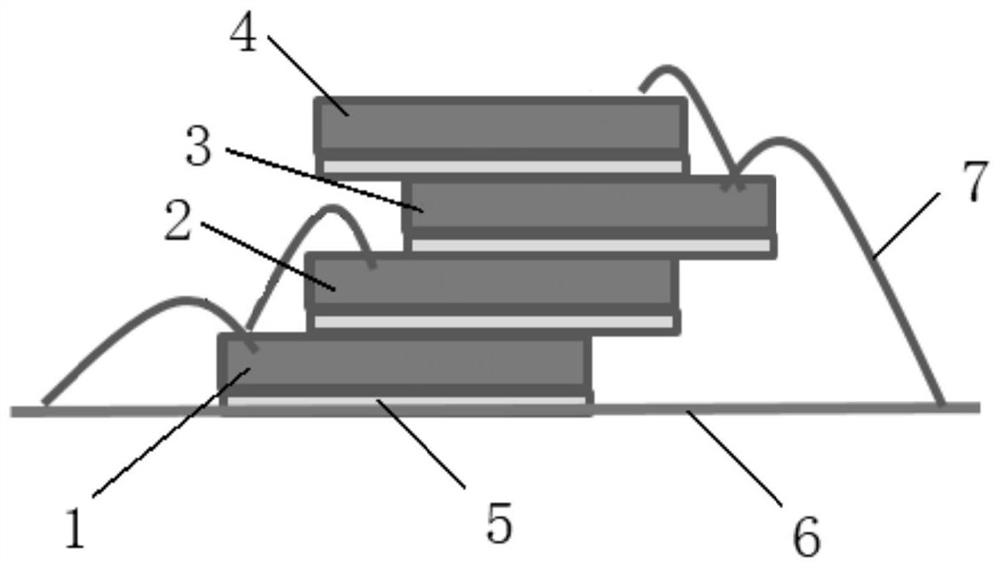
[0031] like image 3 As shown, it is a single-chip stacking package structure in the prior art, including: the first chip 1 is fixed on the substrate 6 through the first adhesive film 5; the second chip 2 is fixed on the first chip 1 through the first adhesive film 5; The three chips 3 are fixed on the second chip 2 by the first adhesive film 5; the second chip 4 is fixed on the third chip 3 by the first adhesive film 5; the first chip 1 and the substrate 6 are electrically connected by the gold wires 7; The second chip 2 and the first chip 1 are electrically connected through the gold wire 7 ; the third chip 3 and the second chip 2 are electrically connected through the gold wire 7 ; the fourth chip 4 and the third chip 3 are electrically connected through the gold wire 7 .
[0032] like Figure 4 As shown, it is a single-chip stack packaging method in the prior art, including:
[0033] Scribing process: After the wafer 11 is supplied, the wafer 11 is diced to form a dicin...
Embodiment 1
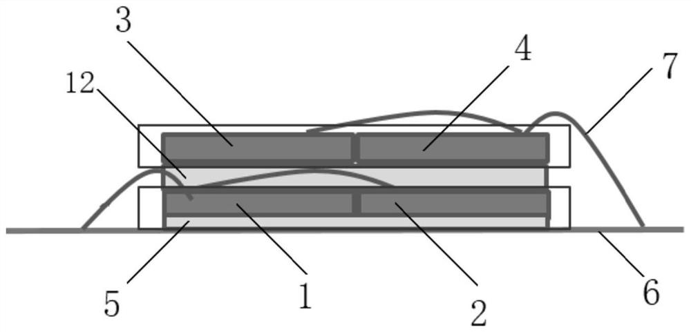
[0038] like figure 1 As shown, a dual-chip stacking package structure includes:
[0039] substrate 6;
[0040] The first chip 1, the second chip 2, the third chip 3 and the fourth chip 4, the first chip 1 and the second chip 2 are cut into a whole; the third chip 3 and the fourth chip 4 are cut into a whole; the first chip 1 and the second chip 2 are cut into a whole; The whole cut of the chip 1 and the second chip 2 is fixed on the substrate 6 by the first adhesive film 5; Chip 2 is cut as a whole;
[0041] The package body is disposed on the substrate 6, and the first chip 1, the second chip 2, the third chip 3 and the fourth chip 4 are packaged in the package body.
[0042] The first chip 1 and the second chip 2 are electrically connected by a gold wire 7; the first chip 1 and the substrate 6 are electrically connected by a gold wire 7; the third chip 3 and the fourth chip 4 are electrically connected by a gold wire 7 is electrically connected; the fourth chip 4 and the...
Embodiment 2
[0048] A two-chip stack packaging method, comprising:
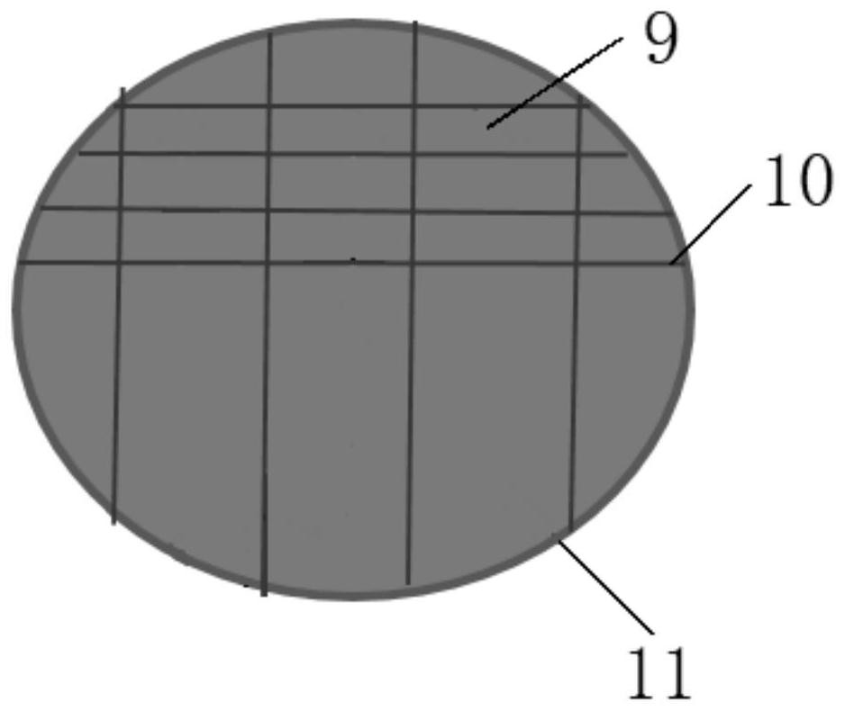
[0049] like figure 2 As shown, the scribing process: after the wafer 11 is supplied, the wafer 11 is scribed horizontally and vertically to form a dicing road 10, and a plurality of double chips 9 are formed by cutting to form a plurality of two chips connected together; reduce the vertical dicing road 10. The hourly output is increased by about 25%; the double chip 9 includes the entire cutting of the first chip 1 and the second chip 2, and the first chip 1 and the second chip 2 do not need to be cut. The whole cut of the first chip 1 and the second chip 2 and the cut whole of the third chip 3 and the fourth chip 4 are all double chips.
[0050] Core loading and wire bonding process: Grab the double chips 9, and only grab the first chip 1 and the second chip 2 once. The prior art needs to grab the first chip 1 and the second chip 2 respectively. Take, the hourly output is increased by about 50%;
[0051] Grab the whole...
PUM
| Property | Measurement | Unit |
|---|---|---|
| Thickness | aaaaa | aaaaa |
| Thickness | aaaaa | aaaaa |
Abstract
Description
Claims
Application Information
 - R&D Engineer
- R&D Manager
- IP Professional
- Industry Leading Data Capabilities
- Powerful AI technology
- Patent DNA Extraction
Browse by: Latest US Patents, China's latest patents, Technical Efficacy Thesaurus, Application Domain, Technology Topic, Popular Technical Reports.
© 2024 PatSnap. All rights reserved.Legal|Privacy policy|Modern Slavery Act Transparency Statement|Sitemap|About US| Contact US: help@patsnap.com


