Wafer-level system packaging structure and method
A system packaging and wafer-level technology, applied in the direction of microstructure technology, microstructure devices, manufacturing microstructure devices, etc., can solve the problems of large package size, low packaging efficiency, and difficult process, so as to enhance mechanical strength and improve Packaging efficiency, the effect of simplifying the process flow
- Summary
- Abstract
- Description
- Claims
- Application Information
AI Technical Summary
Problems solved by technology
Method used
Image

Examples
Embodiment 1
[0030] This embodiment 1 provides a wafer-level system packaging method, including the following steps:
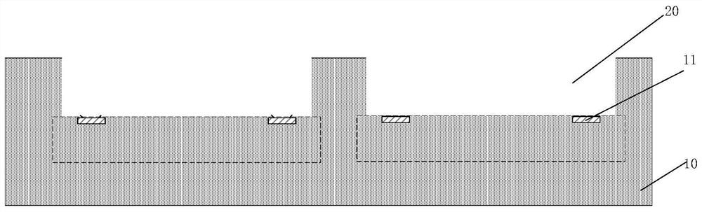
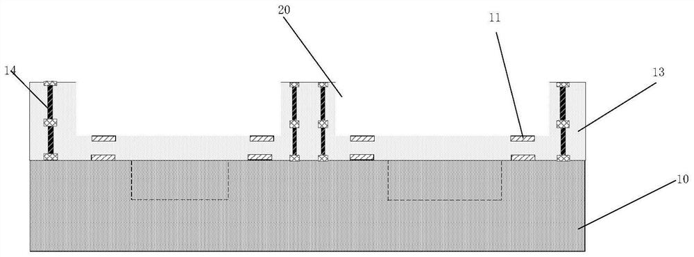
[0031] S01: Provide a device wafer, the surface of the device wafer has a plurality of exposed first pads, the surface of the device wafer forms a first cavity, and at least part of the first pads are located in the first below the cavity;
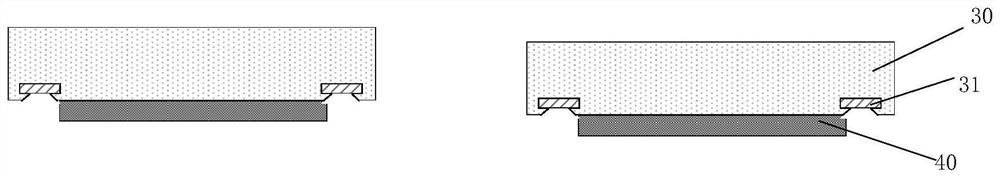
[0032] S02: Provide a first chip, the surface of the first chip has a plurality of exposed second pads, the first chip is embedded in the first cavity and bonded to the device wafer, the the first pad is opposite to the second pad to form a gap;
[0033] S03: A first conductive bump is formed in the gap by an electroplating process, and the first bonding pad and the second bonding pad are electrically connected through the first conductive bump.
[0034] It should be noted that the SON in this specification does not represent the order of the manufacturing processes.
[0035] Figure 1 to Figure 5 A schematic diagram of the structu...
Embodiment 2
[0078] refer to Figure 9 , which is different from Embodiment 1: the backside of the device wafer 10 further includes a third pad 12 , and the third pad 12 is located on the interconnect structure in the device wafer 10 and on the surface of the second chip 80 . The formed fourth pads 81 are electrically connected, the third pads 12 and the fourth pads 81 are arranged opposite to each other, and are formed between the third pads 12 and the fourth pads 81 during the electroplating process The second conductive bumps 90 . In other embodiments, before or after the first conductive bumps 11 are formed, the third pads 12 and the fourth pads 81 may be connected by conductive materials such as solder balls and conductive pillars.
[0079] The exposed area of the third pad 12 or the fourth pad 81 is 5-200 square microns. Within this range, the pad can be in sufficient contact with the electroplating solution to avoid the influence of insufficient contact between the pad and the el...
Embodiment 3
[0081] refer to Figure 10 , the difference from Embodiment 1 is that a third chip 60 is bonded on the first chip 30 , and the third chip 60 is electrically connected to the first chip 30 . Specifically, the first chip 30 includes a fifth pad 32 on the second surface, and the fifth pad 32 is electrically connected to the first chip. The connection can also be achieved by plugs, which is not limited here. A sixth pad 61 is formed on the surface of the third chip 60, and the fifth pad 32 and the sixth pad 61 are arranged opposite to each other. In the electroplating process, a third conductive bump 70 is formed between the fifth bonding pad 32 and the sixth bonding pad 61; the third chip 60 and the first chip 30 can also be electrically connected through an electroless plating process, for example, refer to Figure 11 , the third chip 60 and the first chip 30 can also be electrically connected through the conductive blocks 71 formed by the ball mounting process. At this time, t...
PUM
| Property | Measurement | Unit |
|---|---|---|
| thickness | aaaaa | aaaaa |
| area | aaaaa | aaaaa |
| thickness | aaaaa | aaaaa |
Abstract
Description
Claims
Application Information
 - Generate Ideas
- Intellectual Property
- Life Sciences
- Materials
- Tech Scout
- Unparalleled Data Quality
- Higher Quality Content
- 60% Fewer Hallucinations
Browse by: Latest US Patents, China's latest patents, Technical Efficacy Thesaurus, Application Domain, Technology Topic, Popular Technical Reports.
© 2025 PatSnap. All rights reserved.Legal|Privacy policy|Modern Slavery Act Transparency Statement|Sitemap|About US| Contact US: help@patsnap.com